Nordic’s nRF54H20 highly integrated multiprotocol SoC can be optimized for either processing efficiency or performance.

Nordic Semiconductor has announced the nRF54H20 multiprotocol system-on-chip (SoC), the first device in the nRF54H Series. The multiprotocol SoC combines the processing efficiency and performance necessary for advanced IoT end products, said Nordic.

Nordic claims that the ultra-low power SoC offers best-in-class multiprotocol radio and state-of-the-art security. Target applications include industrial automation and healthcare monitoring, advanced wearables, smart home devices and other devices using machine learning (ML), edge processing or sensor fusion.

The nRF54H20 SoC features multiple Arm Cortex-M33 processors and multiple RISC-V coprocessors optimized for specific workloads. In addition, other processors in the SoC can assist with application processing to increase the SoC’s overall processing performance. The SoC also reduces design size by replacing multiple external components.

With the processing power needed for advanced IoT applications integrated into a single low-power wireless SoC, the nRF54H20 provides a new design approach for developers. “A separate general-purpose MCU and an additional wireless SoC can be replaced with one compact SoC,” Nordic said. This enables IoT end products that are smaller, consume less energy, and offer less design complexity.

Other features include a reduced battery size or prolonged battery life based on the SoC’s processing efficiency, ultra-low power radio and minimal sleep currents; and a multiprotocol radio with 10-dBm TX power and -100-dBm RX sensitivity for Bluetooth LE and -104 dBm for 802.15.4. Security features include secure boot, secure firmware update, secure storage, and protection against physical attacks.

The processor can be optimized for processing efficiency or performance. Nordic used the EEMBC ULPMark-CoreMark benchmarks for maximum processing efficiency or performance, with CoreMark as the workload, achieving the following scores:

Configured for maximum processing efficiency: ULPMark-CM score of 170 with 515 CoreMark. See “Energy, Best Voltage” column in ULPMark-CM score table.

Configured for maximum processing performance: ULPMark-CM score of 132 with 1290 CoreMark. See “Performance” column in ULPMark-CM score table.

The nRF54H20 offers a combination of processing efficiency and performance, where most processors are optimized for one and not both attributes, said Nordic, allowing designers to take advantage of the combination by dynamically changing between configurations.

The nRF54H20 is currently sampling to select customers.

Microchip’s memBrain nonvolatile in-memory compute technology meets IHWK’s SoC processor for neurotechnology devices at the edge.

Artificial intelligence (AI) use at the edge is growing dramatically as embedded system providers increasingly develop brain chips thanks to advances in artificial intelligence (AI) and machine learning (ML). Microchip Technology, Inc. and Intelligent Hardware Korea (IHWK) are partnering to develop an analog compute platform to accelerate edge AI/ML inferencing for neurotechnology devices.

IHWK is developing a neuromorphic computing platform for neurotechnology devices and field-programmable neuromorphic devices. Silicon Storage Technology (SST), a Microchip Technology subsidiary, announced it will assist in the development of this platform by providing an evaluation system for its SuperFlash memBrain neuromorphic memory solution. The solution is based on Microchip’s nonvolatile memory (NVM), SuperFlash technology, optimized to perform vector matrix multiplication (VMM) for neural networks through an analog in-memory compute approach.

A Sheer Analytics & Insights report forecasts that the global market for neuromorphic computing will reach $780 million by 2028, growing at a 50% annual compound annual rate over the forecast years of 2020 – 2028.

“Neuromorphic computing technology mimics brain processes utilizing hardware that operates key processes within the analog domain,” said Mark Reiten, vice president of SST, Microchip’s licensing business unit. “Operation within the analog domain leverages non-von Neumann architecture to deliver AI-powered features at minimal power consumption. This is a significant improvement over mainstream artificial neural networks that are based on digital hardware and traditional von Neumann architecture. The digital approach consumes multiple orders of magnitude more power than the human brain to achieve similar tasks.”

The memBrain technology evaluation kit enables IHWK to demonstrate the power efficiency of its neuromorphic computing platform for running inferencing algorithms at the edge. The goal is to create an ultra-low-power analog processing unit (APU) for applications such as generative AI models, autonomous cars, medical diagnosis, voice processing, security/surveillance, and commercial drones.

This is the first collaboration between the two companies and the term of the collaboration may be several years. “IHWK intends to use the memBrain demo system that we have provided to experiment with design ideas in order to formulate a go-to-market strategy for the edge computing markets they are assessing,” Reiten said.

Current neural net models for edge inference can require 50 million or more synapses (weights) for processing, which creates a bandwidth bottleneck for off-chip DRAM required by purely digital neural net computing. The memBrain solution stores synaptic weights in the on-chip floating gate in ultra-low-power sub-threshold mode and uses the same memory cells to perform the computations. This provides improvements in power efficiency and system latency. When compared to traditional digital DSP and SRAM/DRAM based approaches, it delivers 10× to 20× lower power usage per inference decision and significantly reduces the overall bill of materials (BOM).

“The synaptic weights are stored in the floating gate memory cell as conductance, which means the cell is used as a programmable resistor,” Reiten explained. “When an input voltage is applied to the cell in the horizontal direction on the bitline and combined with the cell conductance, the output which is measured as current is the multiplication of the input voltage (value 1) with the conductance (value 2). We sum the output current of many cells on the wordline to form a ‘neuron’ in the vertical direction in the array.”

IHWK is also working with Korea Advanced Institute of Science & Technology (KAIST), Daejeon, to develop the APU for device development and Yonsei University, Seoul, for device design assistance. The final APU should optimize system-level algorithms for inferencing and operate between 20-80 TeraOPS per watt — the best performance available for a computing-in-memory solution designed for use in battery-powered devices.

“As to the resulting life span of the battery using the technology, it really depends on the specific target market but the memBrain technology should be able to extend battery life of a product by at least 3× compared with comparably performing digital solutions,” Reiten said.

By using NVM rather than off-chip memory to perform neural network computation and to store weights, the memBrain technology can eliminate the massive data communications bottlenecks otherwise associated with performing AI processing at the edge. IHWK is leveraging the SuperFlash memory’s floating gate cells’ nonvolatility to achieve a new benchmark in low-power edge computing devices, supporting ML inference using advanced ML models.

NXP expands AWS cloud service across the S32 automotive MCU and processor platform, providing flexible cloud connectivity for new vehicle architectures.

NXP Semiconductors has extended its support for secure cloud connectivity across its S32 microcontroller (MCU) and processor vehicle compute platform. Addressing body, zone control and electrification applications, NXP has integrated Amazon Web Services (AWS) cloud services into its S32K3 automotive MCUs that balance performance and power efficiency, while addressing todays and future connectivity security, and safety challenges.

With FreeRTOS libraries supporting AWS IoT Core, the S32K3 with integrated cloud connectivity speeds development time for software-defined vehicles (SDVs). They securely connect to the cloud and deliver vehicle data-driven insights and services and over-the-air (OTA) updates, as well as seamless connectivity between the S32K3 and devices running AWS IoT Greengrass.

NXP said secure cloud connectivity services will fuel future, data-driven automotive experiences as well as revenue streams. The processing of real-time, vehicle-wide data with secure cloud service access and machine learning can further intelligent vehicles that continually improve with over-the-air updates, added the company.

The S32 devices’ software with AWS cloud solution can be used with wireless connectivity technologies such as 4G/5G cellular and Wi-Fi. The S32K3 devices can connect directly to AWS cloud services  or a more powerful S32G vehicle network processor using AWS IoT Core, AWS IoT Greengrass or AWS IoT FleetWise.

Extending AWS connectivity to S32K3 gives automotive OEMs the flexibility to build AWS cloud connectivity into their vehicles regardless of the vehicle architecture used, NXP said. This includes architectures in which the S32K3 acts as an end node or zonal controller and supplements an S32G vehicle network processor. It also includes configurations with multiple S32K devices without an S32G processor but has at least one S32K3 used as a gateway to access AWS cloud services.

The end-to-end vehicle data solution now spans across the automotive processing solutions – S32K3, S32Z/E, S32G2 and S32G3, enabling new in-vehicle and secure cloud services. The scalable S32K3 devices are low-power Arm Cortex-M series-based MCUs, AEC-Q100 qualified with advanced safety and security and software support for automotive and industrial ASIL B/D applications in body, zone control and electrification. They feature dedicated hardware security engine (HSE) and A/B swap capability. OTA firmware updates to the S32K3 are secure, protected and supported by third-party software and a tools ecosystem.

Infineon will demo its first Qi2 wireless charging transmitter reference design kit at OktoberTech Silicon Valley.

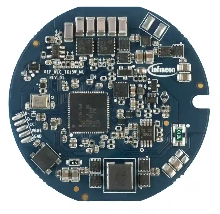
Infineon Technologies AG has introduced its first Qi2 Magnetic Power Profile (MPP) charging transmitter solution, which will be demoed at the company’s OktoberTech Silicon Valley tech collaboration, October 25. The new reference design kit, REF_WLC_TX15W_M1, will demonstrate the capabilities of Infineon’s WLC1 controller. The Qi2 wireless charging transmitter is available for both automotive and consumer applications.

Qi2 is the Wireless Power Consortium’s standard for inductive wireless power transfer. Infineon said the new MPP offers magnet-based fixed positioning with an intuitive user experience for significant benefits in automotive and consumer applications. These include in-cabin wireless charging, smartphones and EarPods cases, portable speakers and healthcare equipment.

The highly integrated reference design kit is form factor optimized with a diameter of less than 43 mm. It is a programmable wireless charging transmitter centered around Infineon’s WLC1 controller. The IC integrates a microcontroller (MCU) with Flash memory, a 4.5-V to 24-VDC input buck-boost controller, inverter gate drivers and factory-trimmed current sensing. It also includes analog protection peripherals, USB PD and LIN as well as serial interfaces for efficient and smart power delivery.

In addition, the 15-W Qi2 MPP solution board is backward compatible with a basic power profile (BPP) that allows receivers without MPP support to wirelessly charge at 5 W. Also provided is a multipath ASK demodulator and adaptive foreign object detection (FOD). Support for the REF_WLC_TX15W_M1 includes code examples in the ModusToolbox to help leverage the IC’s configuration capabilities.

The WLC1 transmitter controllers can be ordered now (the WLC1515 for the automotive package and the WLC1115 for the consumer package). The REF_WLC_TX15W_M1 solution board is available on demand. Visit www.infineon.com/qi2 for more information.

SiTime’s SiT5543 Super-TCXO delivers greater stability and reliability in rugged environments, including aerospace and defense.

SiTime Corp. has launched the ruggedized SiT5543 Super-TCXO, a new member of the Endura MEMS Super-TCXO family, delivering 100× higher reliability for aerospace and defense applications. It also offers 2× lower power consumption and 40% smaller size compared to OCXOs and 20× improvement in stability over quartz TCXOs.

The SiT5543 offers an “unprecedented” ±5-ppb frequency stability over temperature from -40°C to 95°C, compared with quartz TCXOs with a stability of at most ±100 ppb, said SiTime.

The new device also can be used as a replacement for OCXOs in demanding environments where fast temperature transients and vibration are inherent, such as high-speed data communications, military networks, electronic systems and avionics.

The Super-TCXOs enable designers to replace OCXOs, which were previously used to achieve the ±5 ppb stability, without its drawbacks – costly, bulky, fragile and power hungry as well as sensitive to acceleration, shock and vibration, the company said.

The SiT5543 Super-TCXO also is reported to significantly reduce bit error rate, system size and power consumption. Offering a new level of secure, timing-dependent encryption technology, the oscillator protects military radios, GPS receivers, navigation and guidance systems from jamming events. It reduces risk, cycle time and cost, thanks to the MEMS technology, and also reduces design cost and complexity due to its small 7 mm × 5 mm surface-mount footprint, low-power requirements and a unique ability to mitigate the effects of harsh operating conditions, according to SiTime.

Factory-programmable, it eliminates the high cost, risks and delays of custom oscillators, the company said.

Other features include 1-MHz to 60-MHz programmable output frequency, ±0.3 ppb/°C stability over temperature slope, 0.01 ppb/g acceleration sensitivity, 0.5 ppb/day daily aging and low ±150 ppb aging over 20 years, eliminating the need for system-level aging compensation. In addition, it offers 2 seconds to final stability over temperature, an optional ±3200-ppm digital control with I2C, 20,000 g shock survivability and 110 mW typical power consumption at 2.5-V supply.

The SiT5543 is available with I2C digital control for on-the-fly frequency tuning or for advanced user-defined compensation, providing noise-insensitive frequency adjustment with smooth frequency shifts. It can be factory-programmed to a variety of configurations, eliminating long lead time.

Samples of the SiT5543 Super-TCXOs are currently available for qualified customers. Volume production is expected in early 2024.  

Micron claims the industry’s first 8-high 24-GB HBM3 Gen2 with bandwidth greater than 1.2 TB/s for AI data centers.

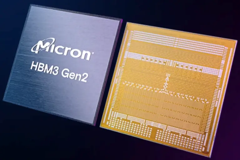
Micron Technology is sampling the industry’s first 8-high 24-GB HBM3 Gen2 memory with bandwidth greater than 1.2 TB/s and pin speed over 9.2 Gbit/s, claiming up to a 50% improvement over current solutions. Boasting a 2.5× performance/watt improvement over earlier generations, the new HBM offering is said to set records for artificial intelligence (AI) data center metrics for performance, capacity and power efficiency. The improvements reduce training times of large language models like GPT-4, deliver efficient infrastructure use for AI inference and lower total cost of ownership (TCO).

At the heart of Micron’s high-bandwidth memory (HBM) solution is its 1β (1-beta) DRAM process node, enabling a 24-Gb DRAM die to be assembled into an 8-high cube in an industry-standard package dimension. Micron delivers 50% more capacity for a given stack height than competitive solutions, according to the company.

The higher memory capacity results in faster training over current solutions and reduced training time for LLMs by more than 30%, Micron said.

The HBM3 Gen3 performance-to-power ratio and pin speeds manage the extreme power demands of today’s AI data centers, the company said. Improved power efficiency is possible given Micron’s doubling of through-silicon vias (TSVs) over competitive HBM3 offerings, thermal impedance reduction through a 5× increase in metal density and an energy-efficient data path design.

The Micron HBM3 Gen2 memory’s performance is driving cost savings for AI data centers. For example, an installation of 10 million GPUs, every five watts of power savings per HBM cube is estimated to save operational expenses of up to $550 million over five years.

Supporting the effort, TSMC is working with Micron for further evaluation and tests for the next-generation HPC application.

Infineon extends its MOTIX family of MCU embedded power ICs for automotive motor control with a CAN-FD interface for faster communication.

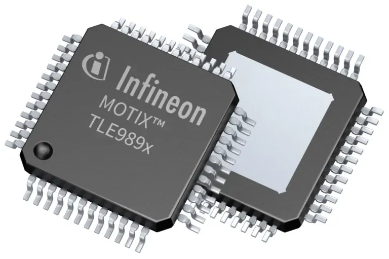
Expanding its portfolio of MOTIX MCU embedded power ICs, Infineon Technologies AG has released the TLE988x and TLE989x bridge driver families. The MOTIX SoCs integrate a gate driver, microcontroller, communication interface and power supply on a single chip for space savings. The new families now feature CAN (FD) as the communication interface.

The MOTIX MCU TLE988x 2-phase bridge driver family and the MOTIX MCU TLE989x 3-phase bridge driver family include multiple devices with Flash memory sizes of up to 256 kB and support temperature ranges (T j max) up to 175°C. The motor driver ICs are AEC Q-100-qualified, making them suited for automotive brushed DC and brushless DC motor control applications in body, comfort and thermal-management applications. They are ISO 26262 (ASIL B) compliant.

A key feature of the bridge driver families is Infineon’s patented Adaptive MOSFET Control algorithm, which compensates for the variation of MOSFET parameters in the system by automatically adjusting the gate current to achieve the required switching. “This allows the system to be optimized in terms of EMI – electromagnetic emissions, slow slew rates – and at the same time, power dissipation – short dead times,” Infineon said.

In addition, the MOSFET control algorithm provides supply chain flexibility by maintaining the same switching behavior across variations in MOSFET production lots or differences between MOSFET suppliers, the company said.

The TLE988x and TLE989x use a B4 or B6 bridge N-channel MOSFET driver, respectively, an Arm Cortex M3 microcontroller, and a CAN (FD) controller and transceiver supporting a communication speed of 2 Mbits/s. The product families also offer about 60% more processing power compared to the TLE987x family and provide functional safety and built-in cybersecurity functions for some variants.

In addition to fast communication, these devices are reported to deliver the highest computing performance thanks to the high system frequency (60 MHz) and its dual Flash enabling read-while-write operation.

The MOTIX MCU TLE988x and TLE989x, housed in a 7 × 7-mm TQFP package, are in production. Two variants in the LQFP package with 64 pins will follow in December 2023.

For design and evaluation, the MOTIX MCU embedded power ICs offer a range of tools that include software, evaluation boards and kits, as well as several simulation, configuration and visualization tools. A 150-W coolant pump reference design is also available. In addition to sample and demo software, commercial software products cover automotive ASPICE-level-qualified motor control libraries including FOC algorithms.

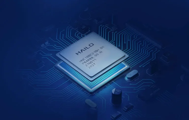
The new Hailo-8 Century and Hailo-8L extend the Hailo-8 AI accelerator platform for high-performance and entry-level applications, respectively.

Addressing the explosion in generative AI-driven applications, Hailo has expanded its Hailo-8 AI accelerator platform portfolio to include a new high-performance Hailo-8 Century PCIe card line that offers 52 to 208 tera operations per second (TOPS) at low power for demanding applications and the Hailo-8L AI accelerator that delivers advanced AI processing to entry-level applications.

The Hailo-8 Century PCIe card line enables real-time, low latency and high efficiency concurrent processing of complex pipelines with multi-streams and multi-models for a broad range of market segments and applications on platforms with a 16-lane PCIe slot. Features include an industrial temperature range of -40°C to 85°C, power efficiency at 400 FPS/W in the ResNet50 benchmark model and a software suite that supports deep learning models and out-of-the-box applications including video management systems that handle many video streams.

In comparison, the Hailo-8L entry-level AI accelerator features up to 13 TOPS and supports entry-level products that require limited AI capacity or lower performance. The accelerator is reported to offer exceptional low-latency and high-efficiency processing and is capable of handling complex pipelines with multiple real-time streams and concurrent processing of multiple models and AI tasks. It is compatible with the Hailo-8 software suite.

Hailo claims that its powerful and cost-efficient solutions bring unmatched AI performance and power efficiency that enable state-of-the-art transformer-based models, such as ViT, CLIP and SAM, at the edge.

Both Hailo-8L and the Hailo-8 Century product lines are available for order. Pricing starts at $249 for the 52 TOPS PCIe card.

AMD’s largest adaptive SoC boasts a range of improvements, which includes a doubling of the programmable logic density for emulation and prototyping.

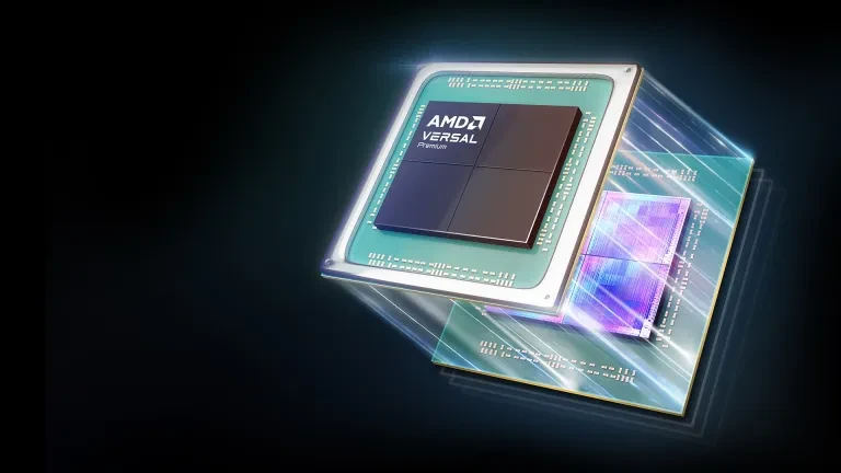
AMD has unveiled the industry’s largest FPGA-based adaptive system-on-chip (SoC), targeting emulation and prototyping applications. The Versal Premium VP1902 chiplet-based adaptive SoC, built on 7-nm process technology, is designed to streamline the verification of complex semiconductor designs to bring them to market faster. It offers twice the capacity over the prior generation, enabling faster validation of ASIC and SoC designs, along with other performance improvements including higher transceiver count and bandwidth as well as faster debugging.

AMD is pushing the limits of the technology to deliver the highest programmable logic capacity and the market that cares the most about that is emulation and prototyping, said Rob Bauer, AMD’s senior product line manager, Versal. “This is all about enabling semiconductor companies to design next-generation chips.”

Emulation and prototyping allow the chip designers to create a digital version or “digital twin” of their chip in hardware, so that they can validate it, identify and iron out the bugs and even develop software upfront before they even have silicon, Bauer said.

Emulation and prototyping challenges

From a technology perspective, the biggest challenges for emulation and prototyping are the chips getting bigger and more complex with chiplet integration and the design costs continuing to climb, making it a problem of a higher magnitude, specifically for verification and software, Bauer said.

However, Bauer said the biggest challenge is looking forward to future ASICs and SoCs and what those will require to create that digital twin. For example, compute (FLOPS) requirements for ML training models roughly followed Moore’s Law, needing to double over 20 months, but in 2010 with deep learning and the large-scale era, including large generative AI models, they now require doubling the compute about every six to nine months, he added.

What this means for emulation and prototyping is the chips that the designers need to emulate are getting much bigger, Bauer continued.

For example, TSMC’s CoWos process has moved from 16 nm to 5 nm over three generations and advanced packaging techniques have moved from a 1× to 3× reticle size interposer, Bauer said. “They’ve been able to achieve a 20× increase in normalized transistor count. This is great in that it means we can pack more compute onto a single device like the MI300 [AMD’s new APU accelerator for AI and HPC], but at the same time there are major challenges when it comes to the integration.”

Techniques like heterogeneous integration or chiplet architectures help drive more performance, but there are major challenges, he added. “We’re not just talking about emulating a single die, or a single piece of silicon. We have to create a digital twin of all these different chiplets and they have to communicate with one another. We also have to verify the communication between them, so that adds some challenges to the emulation and prototyping systems.”

This all drives higher costs. It also means that AI chips and advanced integration require new solutions for emulation and prototyping.

IBS data shows that an advanced 2-nm design is expected to break $700 million in cost, 11.5× more than at 22 nm, Bauer said. Over half of the design cost is for verification and software, he added.

Infineon has added two new F-RAM memory devices in 1-Mbit and 4-Mbit densities to its EXCELON portfolio for automotive data logging.

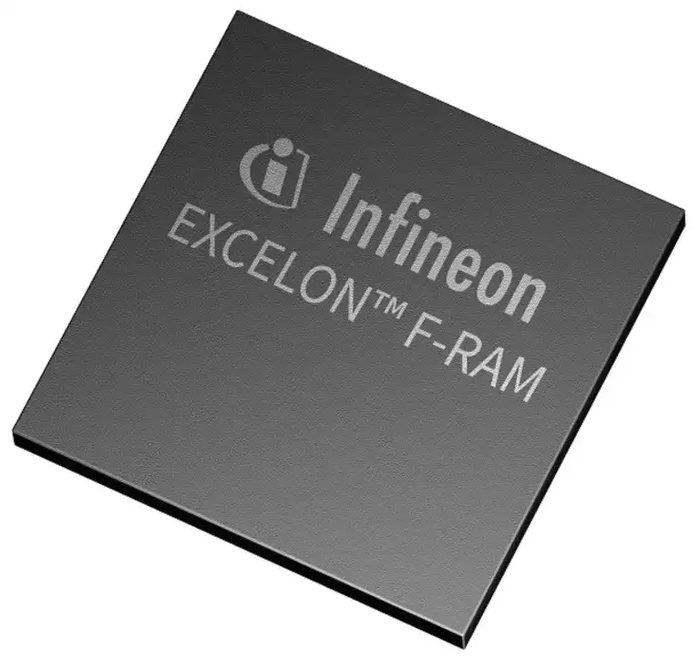
Infineon Technologies AG has expanded its EXCELON Ferroelectric RAM (F-RAM) family with two new memory devices in 1-Mbit and 4-Mbit densities for data logging in automotive event data recorder (EDR) applications that require data stored for decades. The 1-Mbit devices are touted as the industry’s first automotive-qualified serial F-RAMs available.

The EXCELON F-RAM features a zero delay write capability that allows the system data to be captured and recorded up to the last instant before an accident or other user-defined trigger event, said Infineon. It is also designed to retain data for more than 100 years after power loss.

The AEC-Q100 Grade 1-qualified devices operate over an extended temperature range of -40°C to 125°C, joining Infineon’s family of automotive F-RAM products ranging from 4-Kbit up to 16-Mbit densities. They provide fast read/write performance at speeds up to 50 MHz in SPI mode and up to 108 MHz in quad SPI (QSPI) mode, and 10 trillion read/write cycles to support data logging at 10-microsecond intervals for over 20 years.

Other features include the ultra-low power consumption characteristic of the F-RAM, a serial (SPI/QSPI) interface and a 1.8-V to 3.6-V voltage range. The devices are available in a standard 8-pin SOIC package.

The 1-Mbit (CY15B201QN-50SXE) and 4-Mbit (CY15B204QN-40SXE) EXCELON automotive F-RAM devices are now in volume production. A quad SPI interface version of both devices is expected by the end of 2023.