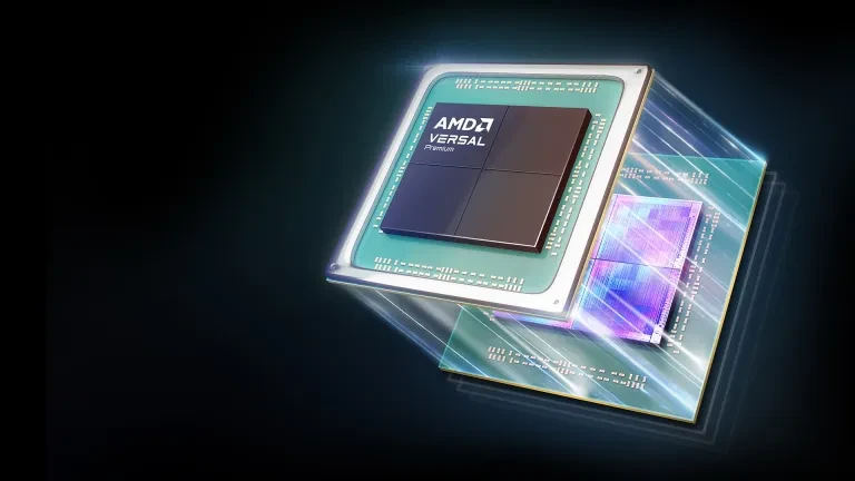
AMD has unveiled the industry’s largest FPGA-based adaptive system-on-chip (SoC), targeting emulation and prototyping applications. The Versal Premium VP1902 chiplet-based adaptive SoC, built on 7-nm process technology, is designed to streamline the verification of complex semiconductor designs to bring them to market faster. It offers twice the capacity over the prior generation, enabling faster validation of ASIC and SoC designs, along with other performance improvements including higher transceiver count and bandwidth as well as faster debugging.
AMD is pushing the limits of the technology to deliver the highest programmable logic capacity and the market that cares the most about that is emulation and prototyping, said Rob Bauer, AMD’s senior product line manager, Versal. “This is all about enabling semiconductor companies to design next-generation chips.”
Emulation and prototyping allow the chip designers to create a digital version or “digital twin” of their chip in hardware, so that they can validate it, identify and iron out the bugs and even develop software upfront before they even have silicon, Bauer said.
Emulation and prototyping challenges
From a technology perspective, the biggest challenges for emulation and prototyping are the chips getting bigger and more complex with chiplet integration and the design costs continuing to climb, making it a problem of a higher magnitude, specifically for verification and software, Bauer said.
However, Bauer said the biggest challenge is looking forward to future ASICs and SoCs and what those will require to create that digital twin. For example, compute (FLOPS) requirements for ML training models roughly followed Moore’s Law, needing to double over 20 months, but in 2010 with deep learning and the large-scale era, including large generative AI models, they now require doubling the compute about every six to nine months, he added.
What this means for emulation and prototyping is the chips that the designers need to emulate are getting much bigger, Bauer continued.
For example, TSMC’s CoWos process has moved from 16 nm to 5 nm over three generations and advanced packaging techniques have moved from a 1× to 3× reticle size interposer, Bauer said. “They’ve been able to achieve a 20× increase in normalized transistor count. This is great in that it means we can pack more compute onto a single device like the MI300 [AMD’s new APU accelerator for AI and HPC], but at the same time there are major challenges when it comes to the integration.”
Techniques like heterogeneous integration or chiplet architectures help drive more performance, but there are major challenges, he added. “We’re not just talking about emulating a single die, or a single piece of silicon. We have to create a digital twin of all these different chiplets and they have to communicate with one another. We also have to verify the communication between them, so that adds some challenges to the emulation and prototyping systems.”
This all drives higher costs. It also means that AI chips and advanced integration require new solutions for emulation and prototyping.
IBS data shows that an advanced 2-nm design is expected to break $700 million in cost, 11.5× more than at 22 nm, Bauer said. Over half of the design cost is for verification and software, he added.


