Bourns, Inc. has launched its first 650 V – 1200 V silicon carbide (SiC) Schottky barrier diodes (SBDs), comprised of six models designed to provide excellent current carrying and thermal capabilities and high power density. The BSD series delivers increased performance and reliability for high-frequency applications.
Developed for designs that need higher efficiency and switching performance, the BSD series devices provide high-efficiency power conversion solutions for high-frequency applications that need to reduce their size and lower system cost. Target applications include telecom/server switched-mode power supplies (SMPS), photovoltaic inverters, PC power and motor drives, for reduced thermal resistance and low power loss.
The six new wide-bandgap diodes offer designers a variety of forward voltage, current and package options including TO220-2, TO247-3, TO252 and DFN8×8. They feature low forward voltage (VF) and high thermal conductivity, designed to increase efficiency and lower power dissipation in 650-V and 1200-V solutions.
The series also features no reverse recovery current to reduce electromagnetic interference (EMI), enabling these SiC SBDs to significantly lower energy losses, said Bourns. Current ratings range from 6-10 A.
The SiC SBDs are currently available. They are RoHS compliant, halogen free, and lead free. They also feature a flame-retardant epoxy potting compound, meeting the UL 94V-0 standard.
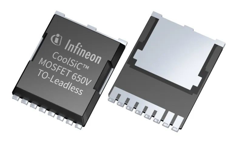
Infineon Technologies Inc. has introduced its 650-V CoolSiC MOSFET in TO leadless (TOLL) packaging, which is designed to optimize performance and reliability for a variety of applications, including those in harsh environments. Applications include SMPS for servers, telecom infrastructure, energy storage systems and battery formation solutions.
The new family’s JEDEC-qualified TOLL package features a low parasitic inductance for higher switching frequency, reduced switching losses and good thermal management. In addition, the compact form factor enables efficient use of the board space, enabling system designers to achieve greater power density.
A key feature of the new device is the inclusion of the innovative .XT interconnect technology to enhance thermal performance by reducing the thermal resistance (Rth) and thermal impedance (Zth). Other features include a gate threshold voltage (VGS(th)) greater than 4 V for robustness against parasitic turn-on and a robust body diode.
Infineon also reported that the SiC-based MOSFET offers the “strongest” gate oxide (GOX), resulting in extremely low failures in time (FIT) rates, high reliability and low losses.
The new portfolio supports a wide driving interval of VGS voltage within the range of -5 V (turn off) to 23 V (turn on), ensuring ease-of-use and compatibility with other SiC MOSFETs and standard MOSFET gate-driver ICs. This results in reduced system complexity, enabling automated assembly and reducing system and production costs.
The 650-V CoolSiC MOSFET in TOLL industrial-grade discretes are available for order in a variety of drain-source on-resistance (RDS(on)) options from 22 to 83 mΩ. The 107 mΩ, 163 mΩ and 260 mΩ versions will be available on-demand.
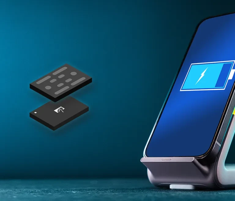
Alpha and Omega Semiconductor Limited (AOS) has unveiled its new MRigidCSP packaging technology for battery management applications. The new packaging is reported to decrease on-resistance, while increasing mechanical strength. It will be initially available for the AOCR33105E, a 12-V common-drain dual N-channel MOSFET. Target battery applications include smartphones, tablets and ultra-thin notebooks.
The MRigidCSP packaging resolves a few key challenges around fast charging, which calls for lower power loss in the battery management circuit.
“As the charging currents increase, ultra-low electrical resistance is needed for improved performance. In standard wafer-level chip scale packages (WL-CSPs), the substrate can be a significant portion of the total resistance when back-to-back MOSFETs are employed in battery management applications,” AOS explained. “A thinner substrate reduces the overall resistance but drastically reduces the package’s mechanical strength.”
AOS said the reduction in mechanical strength can result in more stress during the PCB assembly reflow, which could cause warping or cracking in the die as well as application failure.
The AOCR33105E is designed with the latest trench-power MOSFET technology in a common drain configuration. It features ultra-low on resistance and electrostatic discharge (ESD) protection to improve performance and safety in battery management, such as protection switches and mobile battery charging and discharging circuits. The device is RoHS 2.0 compliant and halogen-free. Click here for more product resources.
The AOCR33105E in the MRigidCSP package is available in production quantities with a lead time of 14-16 weeks. The device is priced at $0.405 in quantities of 1,000.
STMicroelectronics (ST) has launched its TSZ181H1 and dual TSZ182H1 automotive-qualified operational amplifiers (op amps) for automotive and industrial applications. These devices deliver high accuracy and stability over a wide -40°C to 175°C temperature range for use in harsh environments.
The op amps also deliver a very low input offset voltage, typical 3.5 µV at 25°Cm, and input bias current, typical 30 pA at 25°C. ST said the parameters display minimal drift over temperature, with maximum input offset voltage specified as 70 µV at 25°C and 100 µV over the full temperature range. The maximum specified input bias current is 200 pA at 25°C and 225 pA over the full range.
In addition to withstanding harsh environments thanks to their wide operating-temperature range, the TSZ181H1 and TSZ182H1 also can operate for an extended lifetime in applications that require a long mission profile. The devices are AEC-Q100 qualified and provide 4-kV HBM ESD tolerance.
The new op amps can be used for precision signal conditioning without calibration, said ST, which helps simplify end-product manufacturing while providing higher accuracy.
Other specs include a gain bandwidth of 3 MHz, an operating current of just 1 mA at 5 V and a power supply voltage range from 2.2 V to 5.5 V. Both devices have rail-to-rail input and output to maximize usable dynamic range, said ST.
Both op amps are in production and available in SOT23-5 or SO8 packages. Pricing starts at $1.58 for the TSZ181H1 and $2.66 for the TSZ182H1 dual op amp.
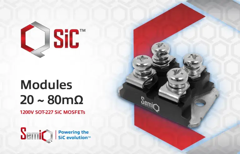
SemiQ has expanded its portfolio of QSiC silicon carbide (SiC) modules with the launch of a family of 1,200-V MOSFETs that pairs with or without 1,200-V SiC Schottky diodes in a SOT-227 package. The new 1,200-V SiC modules offer enhanced performance, delivering higher power densities and more streamlined design configurations, said the company.
The QSiC modules feature high breakdown voltage (>1,400 V), high-temperature operation (Tj = 175°C), and low Rds(On) shift over the full operating temperature range. They also provide high gate-oxide stability and gate-oxide lifetime, avalanche (UIS) ruggedness and extended short-circuit withstand times, SemiQ said.
Target markets for the new ultra-efficient QSiC SiC modules and existing SOT-227 SiC SBD modules include EV charging, on-board chargers (OBCs), DC/DC converters, E-compressors, fuel cell converters, medical power supplies, energy storage systems, solar and wind energy systems, data-center power supplies, UPS/PFC circuits and other automotive and industrial power applications.
SemiQ said all of the new QSiC modules are tested at wafer-level gate burn-in to provide high-quality gate oxide with a stable gate threshold voltage. In addition to the burn-in test, which helps to stabilize the extrinsic failure rate, stress tests such as gate stress and high-temperature reverse bias (HTRB) drain stress, as well as high humidity, high voltage and high temperature ensure industrial-grade quality levels, said the company.
Texas Instruments Inc. (TI) has expanded its low-power gallium nitride (GaN) portfolio, with a new family of GaN field-effect transistors (FETs). These GaN FET devices can improve power density and system efficiency, while shrinking the size of AC/DC consumer power electronics and industrial systems.
They can reduce the solution size of a typical 67-W power adapter by as much as 50% compared to silicon-based solutions, according to TI.
TI’s portfolio of GaN FETs with integrated gate drivers also help solve common thermal design challenges, said the company, and keep adapters cooler while pushing more power in a smaller footprint.
“With the expansion of our portfolio, designers can bring the power-density benefits of low-power GaN technology to more applications that consumers use every day, such as mobile phone and laptop adapters, TV power-supply units, and USB wall outlets,” said Kannan Soundarapandian, TI’s general manager of High Voltage Power, in a statement.
The new portfolio of GaN FETs with integrated gate drivers, includes the LMG3622, LMG3624 and LMG3626, claiming the industry’s most accurate integrated current sensing. This functionality eliminates the need for an external shunt resistor and reduces associated power losses by as much as 94% when compared to traditional current-sensing circuits used with discrete GaN and silicon FETs, TI said.
These GaN FETs with integrated gate drivers enable faster switching speeds, which helps with overheating in adapters. For example, by using these devices, designers can achieve up to a 94% system efficiency for <75-W AC/DC applications or above 95% system efficiency for >75-W AC/DC applications.
These devices are optimized for common topologies in AC/DC power conversion, such as quasi-resonant flyback, asymmetrical half-bridge flyback, inductor-inductor-converter, totem-pole power factor correction and active clamp flyback.
Production quantities of the LMG3622 and LMG3626 and pre-production quantities of the LMG3624 are available for purchase now on TI.com/GaN. Available in an 8 × 5.3-mm, 38-pin quad flat no-lead package, pricing starts at $3.18 in quantities of 1,000. Prices start at $250 for evaluation modules, including the LMG3624EVM-081. Pin-to-pin devices without integrated current sensing, LMG3612 and LMG3616, are also available.
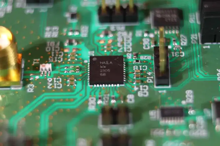
HaiLa Technologies Inc. announced the availability of the BSC2000 backscatter chip and RF evaluation chip development and demonstration kits. Collaborating with Presto Engineering, the companies developed what they claim is the first complete analog and digital implementation of HaiLa’s passive backscatter technology adapted to Wi-Fi RF bands.
Touted as the first Wi-Fi-based “extreme-low-power” backscatter chip, Presto Engineering said pushing the limit of IoT power efficiency is a game changer for mitigating battery cost and waste. It also supports a key industry initiative to help reduce the carbon footprint of connected devices.
HaiLa’s passive backscatter foundational technology is protocol-agnostic. The company focused its first adaptation on Wi-Fi as a key infrastructure enabler for IoT deployment.
The BSC2000 features an SPI interface for seamless connectivity to a range of IoT devices such as multi-channel temperature and humidity sensors. It provides a path to extreme-low power in IoT devices used in building, home, and industrial automation; consumer electronics and wearables; smart transportation, agriculture, medical and automotive markets.
For its part of the collaboration, Presto brought substantial experience in ultra-low-power RFID and NFC, enabling HaiLa to complement its team with resources embedded into the development process, Haila said.
The BSC2000 is currently sampling. The BSC2000 Development Kit supports a comprehensive evaluation of the BSC2000 RF Evaluation Chip. An accompanying BSC2000 Wi-Fi backscatter tag demonstration kit illustrates tag form factor and extended tag battery life based on a CR2032 coin cell battery. HaiLa is demonstrating the BSC2000 at CES, LVCC, West Hall, booth 6300.
Ambarella, Inc. has demonstrated multi-modal large language models (LLMs) running on its new N1 SoC series at a fraction of the power-per-inference of leading GPU solutions. The company will initially offer optimized generative AI processing capabilities on its mid- to high-end SoCs, from the CV72 that delivers on-device performance under 5 W to the new N1 series for server-grade performance under 50 W.
Ambarella claims that its complete SoC solutions are up to 3× more power-efficient per generated token compared to GPUs and other accelerators.
The N1 series of SoCs, based on the company’s CV3-HD architecture initially developed for autonomous driving applications, runs multi-modal LLMs in an extremely low power footprint, such as Llama2-13B with up to 25 output tokens per second in single-streaming mode at under 50 W of power. The new solution helps OEMs to deploy generative AI into any power-sensitive application.
Ambarella plans to bring generative AI to edge endpoint devices and on-premises hardware applications including video security analysis, robotics and industrial. “Virtually every edge application will get enhanced by generative AI in the next 18 months,” said Omdia’s principal analyst, Advanced Computing, Alexander Harrowell, in a statement.
Harrowell explained that when moving genAI workloads to the edge, it is all about performance/watt and integration with the existing edge ecosystem, rather than just raw throughput.
Generative AI can deliver new functions to the edge that were not previously possible, Ambarella said. The company’s AI SoCs are supported by its new Cooper Developer Platform that provides seamless integration of software, hardware, fine-tuned AI models and services. This platform offers a modular and prepackaged suite of hardware and software development tools.
Ambarella has pre-ported and optimized popular LLMs, such as Llama-2 and the Large Language and Video Assistant (LLava) model, running on N1 for multi-modal vision analysis of up to 32 camera sources. These pre-trained and fine-tuned models will be available for partners to download from the Cooper Model Garden.
Examples of the on-device LLM and multi-modal processing include smart contextual searches of security footage; robots that are controllable with natural language commands, and AI helpers that perform anything from code generation to text and image generation.
The local processing, resulting from Ambarella’s solutions, suits application-specific LLMs, fine-tuned on the edge for individual scenarios rather than using a traditional server approach with bigger and power-hungry LLMs for every use case.
Renesas Electronics has introduced its lowest power consumption and smallest multi-core (Cortex-M33, Cortex-M0+) Bluetooth Low Energy (LE) system-on-chip (SoC). The DA14592 BLE SoC, balancing tradeoffs between on-chip memory and SoC die size, targets applications such as connected medical, asset tracking, human interface devices, metering, PoS readers and “crowd-sourced location” (CSL) tracking.
The solution’s new low-power mode is reported to offer “world-class” 2.3-mA radio transmit current at 0 dBm and 1.2-mA radio receive current. Supporting an ultra-low hibernation current of 90 nA, the DA14592 extends shelf-life for end-products shipped battery connected and supports ultra-low active current at 34 µA/MHz for products that require significant application processing.
From a solution cost perspective, the DA14592 requires only six external components, Renesas said. Operating from only a system clock and a highly accurate on-chip RCX, the device eliminates the need for a sleep mode crystal in most applications. The small footprint DA14592 also includes a high-precision, sigma-delta ADC, up to 32 GPIOs. Unlike other SoCs in its class, it offers a QSPI supporting external memory (Flash or RAM) expansion for applications that require extra memory.
All external components required to implement a Bluetooth LE solution is integrated into the DA14592MOD module for the fastest time-to-market and reduced overall project cost, Renesas said. The module delivers design flexibility by routing the DA14592’s functions to the outside of the module and using castellated pins for easy and low-cost module attachment.
A key application for the DA14592 and DA14592MOD is crowd-sourced locationing, or CSL, a market projected to reach over $29 billion in North America by 2031. Renesas will offer reference designs that help accelerate tag designs and enable manufacturers of lost or stolen products to easily attach the DA14592, making their product globally locatable. In addition, the DA14592MOD removes the need for worldwide regulatory certifications, reducing development costs and further accelerating time-to-market, the company said.
Offered in WLCSP (3.32 × 2.48 mm) and FCQFN (5.1 × 4.3 mm) packages, the DA14592 is currently in mass production and the DA14592MOD is expected to receive worldwide regulatory certifications in the second quarter of 2024. Renesas has combined the new DA14592 with a variety of its compatible devices from its portfolio to offer technically vetted Winning Combinations, including the Instrument Panel for Light Electric Vehicles.
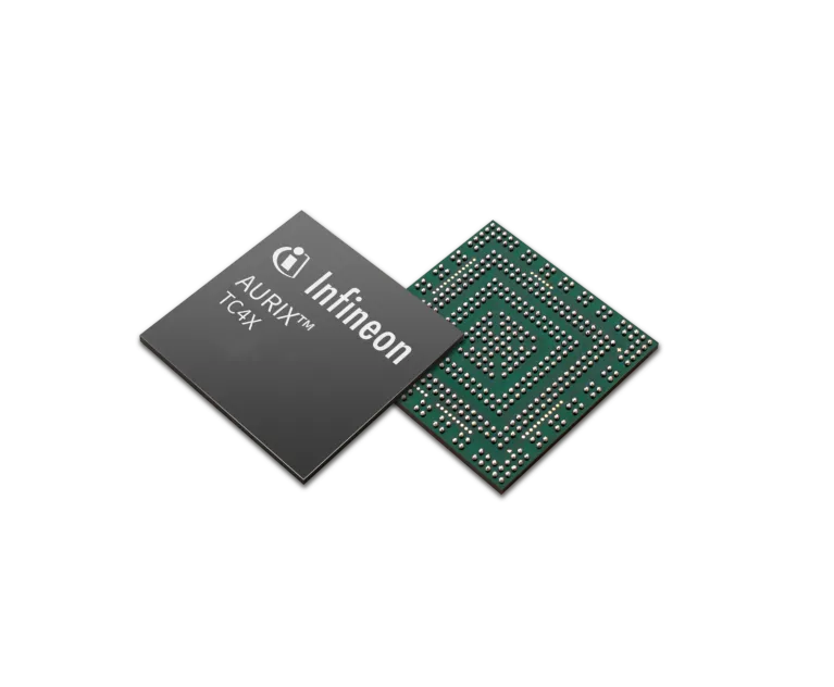
Infineon Technologies AG and Aurora Labs have debuted a new set of AI-based solutions at CES 2024, which are designed to improve the long-term reliability and safety of critical automotive components, including steering, braking and airbags. These automotive safety solutions leverage Aurora Labs’ vehicle software Line-of-Code Intelligence (LOCI) AI technology and Infineon’s 32-bit TriCore AURIX TC4x family of microcontrollers (MCUs).
Targeting improved predictive maintenance for the automotive industry, the new solution is centered on Infineon’s AURIX TC4x family of MCUs with real-time safety and security performance with Aurora Labs’ AI- and ML-based features implemented in the AURIX TC4x parallel processing unit (PPU), a purpose-built AI accelerator. These features do not share any resources with the OEM applications running on the CPU, Infineon said.
The partnership has resulted in a solution that enables AI-driven automated processes throughout the software lifecycle of an automobile to deliver safer vehicle systems. It supports real-time monitoring and response to software failures at the MCU- and ECU-level according to WP29 requirements and helps prevent malicious attacks and hardware safety failure by protecting applications and over-the-air (OTA) updates.
“With the combination of Infineon’s proven AURIX MCUs, along with Aurora Labs’ software to prevent silent data corruption and software misbehavior in chipsets, our new solution gives car manufacturers and drivers an extended level of safety confidence for critical automotive applications such as steering, braking and airbags, said Thomas Schneid, senior director Software, Partner and Ecosystem Management of Infineon, in a statement.
Infineon and Aurora Labs’ new predictive safety maintenance solution is available now. The AURIX MCUs are designed for next-generation eMobility, advanced driver assistance (ADAS), automotive E/E architectures and artificial intelligence (AI) applications.