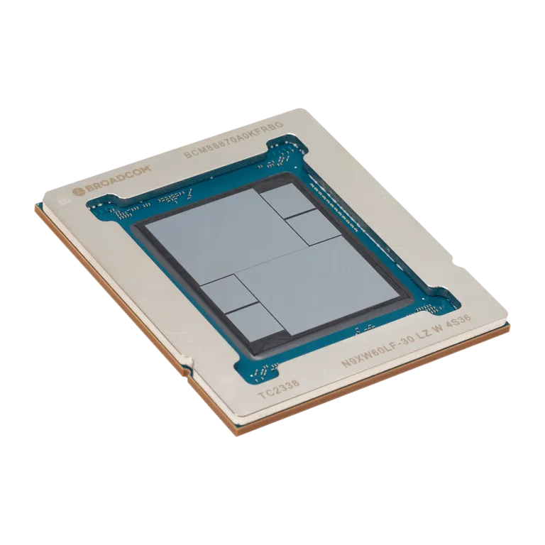
Broadcom’s Trident 5-X12 Ethernet switch doubles bandwidth and reduces power, adding a neural network for telemetry, security and traffic engineering.

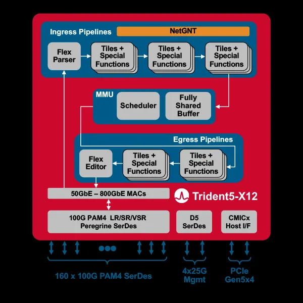
Broadcom Inc. has announced a neural-network inference engine, the networking general-purpose neural-network traffic-analyzer (NetGNT) housed on a new, software-programmable and field-upgradable Trident 5-X12 Ethernet switch. The company claims it is the industry’s first Ethernet switch with an on-chip neural network.

Target applications include data-center programmable top-of-rack (ToR), data center leaf/spine, switch blade in a server chassis, line card and fabric in a switch chassis, border/data-center interconnect (DCI) and edge compute data center disaggregation.

The Trident 5-X12 chip uses 25% less power per 400G port compared to the Trident 4-X9 and its 16.0 terabits/second of bandwidth is double that of the Trident 4-X9. It supports the transition to next-generation CPU and GPU servers using 400G NICs and enables new capabilities and improved network efficiency and performance. It also adds support for 800G ports, allowing direct connection to Broadcom’s Tomahawk 5, used as the spine/fabric in the newest compute and AI/ML data centers.

The chip is positioned to enable a 1RU data center ToR, supporting 48×200G downlink ports and 8×800G uplink ports. Enhanced telemetry capabilities allow deeper real-time insights into network operations, which can then be used to train the NetGNT. Support for Enterprise SONiC and SAI promote fast, seamless integration into data center operations frameworks, Broadcom said.

The chip also features robust connectivity using up to 160 instances of the high-performing, longest-reach 100G PAM-4 integrated SerDes core that enables a variety of optical and direct attached copper (DAC) links with up to a 4-meter DAC reach. It is cost- and power-optimized for next-generation data center and campus networks and supports 400G ToRs with a compiler-programmable architecture. The NetGNT is an ML inference engine and can be trained to look for different types of traffic patterns that span the entire chip.

Broadcom is currently shipping Trident 5-X12 devices to qualified customers.

Broadcom’s Qumran3D single-chip router addresses increased bandwidth and security demands driven by AI, mobile edge and other high-data deployments.

Broadcom is now shipping the next-generation of its StrataDNX family of single-chip routers. The new Qumran3D single-chip router targets carrier and cloud service providers facing bandwidth, subscriber and services growth.

The Ethernet switch router chip, claimed as the industry’s first built on 5 nm, offers 25.6 terabits per second (Tbits/s) of routing in a fixed form factor. A routing solution, using a single Qumran3D, is expected to save up to 66% more energy and 80% more rack space than previous generations, according to Broadcom.

Delivering a high-performance, low-power and security-rich networking solution , the Qumran3D meets bandwidth and security requirements driven by AI, mobile edge and other high-data deployment, Broadcom said. Applications include core, edge, peering and DCI routers, as well as aggregation systems.

Features include high-speed, high-density port interfaces up to 800GE; a processing pipe addressing any carrier and cloud requirements and futureproofing via Elastic Pipe; carrier-grade hierarchical traffic manager, HBM packet memory and massive on-chip forwarding databases that eliminate the need for companion devices.

Another key feature is dedicated on-chip processing and buffering, with large-scale forwarding, strong security and native line-rate MACsec encryption on all ports. The embedded forwarding databases meet the required scale for any routing environment, with sufficient headroom for continued growth of subscribers and services in the coming decade, according to Broadcom.

In addition, the company reports that theQumran3D’s 256 links of 100G PAM-4 SerDes enable a 25% to 50% reduction in the optical transceivers’ power consumption for the cluster interconnect using linear drive optics. It also supports emerging 800ZR+ optics for DCI and IP over DWDM.

On the security front, the router’s large-scale on-chip policy tables provide privacy and protection to the network and its subscribers. Flexible policy engines, IPsec for connection security and MACsec for line-rate encryption deliver protection to subscribers with millions of private connections, without a performance compromise, Broadcom said.

Broadcom is currently shipping Qumran3D devices to qualified customers.

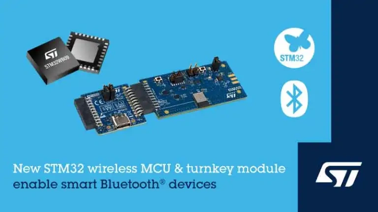
STMicroelectronics simplifies the design of smart Bluetooth devices with a new wireless MCU and turnkey module.

STMicroelectronics has introduced two new products—a wireless microcontroller (MCU) and wireless module—that are designed to simplify the design of short-range wireless connectivity devices. Aimed at different skill sets, the STM32WB1MMC wireless module targets designers without extensive RF engineering skills and resources, while the STM32WB09 wireless MCU is suited for skilled designers.

ST said the latest Bluetooth specification opens up new opportunities for smarter wireless devices, including wireless beacons and other devices that can calculate their location indoors with centimeter accuracy.

The STM32WB09 wireless MCU includes all the processing power and Bluetooth RF technology needed in one chip and is available with a tiny chip-scale package option. It is built on the Arm Cortex-M0+ single-core architecture with “generous” on-chip memory. The peripherals and memory are tailored for applications such as wireless sensing, connected wearables and remote control. The SoC also can be used for warehouse inventory management systems, smart meters, access controls and medical devices such as disposable sensors.

The all-in-one STM32WB1MMC wireless module makes wireless connectivity easier with a certified wireless MCU pre-integrated with external components needed for the radio system, as well as the latest Bluetooth software. It is built on the STM32WB15 MCU with 320 KB Flash and 48 KB RAM and comes with Bluetooth Low Energy 5.4 certification and worldwide radio-equipment approvals. Engineers have access to a full reference design in an LGA package as well as ST’s PC-based design tools, software and sample code to speed up application development.

ST also introduced the B-WB1M-WPAN1 evaluation board for building prototypes with the STM32WB1MMC MCU module. The board also includes movement, temperature and barometric-pressure sensors that can be incorporated into the system. Other features include an industry-standard connector for attaching an external antenna, flexible power supply options, user LED and reset pushbuttons. Designers can use the STM32Cube ecosystem with the board for easier power consumption testing with the STM32CubeMX calculator and RF testing with the STM32CubeMonRF software tool.

The STM32WB09 wireless MCU, STM32WB1MMC turnkey wireless module, and B-WB1M-WPAN1 module evaluation board are all in production now. Pricing for the STM32WB09 starts from $1.36 in the QFN32 package. The STM32WB1MMC modules are priced at $5.32 for orders of 10,000 units. The B-WB1M-WPAN1 is available from www.st.com and distributors, from $30.00.

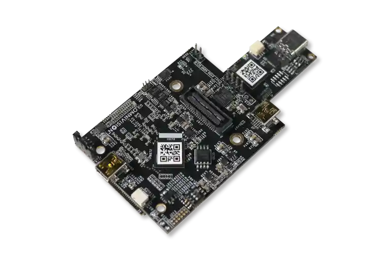
Omnivision’s OVMed OH0131 image signal processor for endoscopes supports the company’s up to 2-MP resolution medical image sensors.

Omnivision has expanded its OVMed family with the introduction of the OH0131 image signal processor (ISP) for reusable and disposable endoscopes connected to handheld tablet consoles or camera control units (CCUs). The ISP supports Omnivision’s medical image sensors, up to 2-megapixel (MP) resolution, including the OCHTA,  OVM6946, OCHFA, OCHSA and OCH2B.

By providing the medical-grade image sensors with wafer-level optics along with the cable and ISP from one vendor, it simplifies the supply chain for medical OEMs, Omnivision said.

The OH0131 ISP is based on an ASIC system-on-chip (SoC) for high image quality and high reliability as well as cost-effectiveness. It supports Omnivision’s proprietary AntLinx CMOS chip-on-tip endoscopy imaging interface and MIPI interfaces. It can integrate with any MIPI-input post-processing board by an SoC, FPGA or x86 platform to build custom CCUs or handheld tablet consoles.

Omnivision said the OH0131 kernel features the latest state-of-the-art image pre-processing algorithms that support brightness, contrast, saturation, sharpness, hue, white balance and gamma adjustment with advanced noise reduction. Post processing performed by a third-party partner using an SoC or FPGA can target features such as LED drivers, patient isolation, high dynamic range, image rotation, image mask/onscreen display, H.264 compression, high-definition multimedia interface and Wi-Fi output.

The OVMed OH0131 image signal processor is available now. The ISP will undergo IEC 60601 EMC and EMI pre-scan testing. The miniature board measures 63 mm × 51 mm.

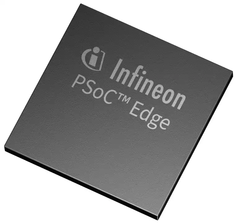
Infineon launches its new family of PSoC Edge MCUs for power-efficient machine learning at the edge.

Infineon Technologies AG has released a new family of PSoC microcontrollers (MCUs) for power-efficient machine learning (ML) at the edge. The new PSoC Edge are Arm Cortex-based MCUs that enable next-generation responsive compute and control applications and feature hardware-assisted ML acceleration.

The PSoC Edge MCU family features ML-enhanced sensing, low power, secured and advanced HMI performance. Privacy and safety protection is provided through Infineon’s Edge Protect technologies. Applications include IoT and industrial segments such as smart home, security systems, wearables, robotics and HMI applications.

The new MCUs enable end products to be more intelligent and intuitively usable, lowering the barrier in human-machine interaction and adding contextual awareness to applications, Infineon said. The enhanced intelligence extends support for advanced graphics, voice, audio and vision-based applications to the existing PSoC portfolio. It also enables easy migration of applications within the family and an upgrade path from existing designs.

Offering scalable power and performance, extensive HMI capabilities and security, the PSoC MCUs are based on high performance Arm Cortex-M55, including Helium DSP support paired with Arm Ethos-U55 and Cortex-M33, combined with Infineon’s ultra-low-power NNLite hardware accelerator that accelerates neural networks used in ML and AI. The family provides on-chip memories, including non-volatile RRAM, and high speed, secured external memory support. It also enables software reuse and portability.

For development support, Infineon’s ModusToolbox software provides development tools, libraries and embedded runtime assets for a range of applications including industrial, smart home and wearables. Imagimob Studio AI solution, an edge AI development platform, is integrated into the ModusToolbox, providing end-to-end ML development. Starter projects and Imagimob’s Ready Models, with PSoC Edge, enable the deployment of ML models for the edge.

PSoC Edge is currently available for early access customers.

Silicon Labs expands microcontroller offerings with new BB5 family of 8-bit MCUs for space-constrained applications.

Silicon Labs has unveiled the BB5 family of 8-bit microcontrollers (MCUs), targeting space-constrained and low-cost applications that don’t require a 32-bit solution. Optimized for price and performance, the multi-purpose EFM8BB50 integrates advanced analog and communication peripherals into small packages.

Key features include an 8051 core, up to 12 multi-function 5-V capable I/O pins, a 1 × 12-bit analog-to-digital converter, an integrated temperature sensor, 3-channel PCA with pulse-width modulation (PWM), a 3-channel PWM engine, 4 × 16-bit timers, 2 × 8-bit timers and QFN packages as small as 2 × 2 mm.

The BB5 8-bit MCUs are suited for battery-powered applications like power tools, handheld kitchen tools and children’s toys, supporting voltage options from 1.7 to 5.5 V, allowing them to last for years in the field on a coin-cell battery, according to the company. Other embedded applications include LED/lighting control, industrial automation, appliances, motor control and consumer electronics.

In addition, the company claims the BB5 family includes “the most powerful 8-bit MCUs” with the 50-MHz core frequency delivering 36% higher compute power than any other general 8-bit MCU.

Available in multiple variants, the BB50 is the smallest option housed in a 2 × 2 mm package. The BB51 and BB52 feature a 3 × 3-mm package with more peripheral options and increased analog functionality. In some applications, the BB52 offers a higher price/performance when compared to competitive 32-bit MCUs, according to Silicon Labs. Click here for the data sheet.

The BB5 MCUs leverage Silicon Labs’ Simplicity Studio, which eliminates design process complexity and shortens development cycles. This enables both 8-bit and 32-bit MCUs to share a single development platform, which has been challenging for developers, said the company, since most 8-bit and 32-bit devices use different development tools.

Silicon Labs also offers the EFM8 BB50 8-bit MCU Explorer Kit, BB50-EK2702A, as an evaluation starting point for the new MCUs. It provides Qwiic and MikroE connectors for rapid prototyping and an on-board debugger.

The Synaptics SYN43711 wireless SoC reduces cost, space, power and complexity for secure IoT consumer and industrial devices.

Synaptics Inc. has expanded its wireless connectivity portfolio for consumer and industrial IoT applications, with the launch of the SYNA43711 Wi-Fi 6E and Bluetooth 5.3 combo system on chip (SoC). The wireless SoC addresses high-performance use cases that require high Wi-Fi throughput and range.

According to Synaptics, by integrating the Wi-Fi 6/6E and Bluetooth 5.3 radios on a single SoC, it reduces the space, cost, power, complexity and time to market of wireless IoT devices. Applications include high-end home appliances, surveillance cameras, robots and other consumer, industrial and enterprise systems.

The single-stream (1×1 antenna arrangement with a throughput of 600 Mbits/s) device complements Synaptics’ dual-stream (2×2, 1,200 Mbits/s) SYN43756E and Triple Combo SYN438x series, providing a more cost-effective and smaller form factor option. The Wi-Fi radio is IEEE 802.11ax compliant with legacy support for 802.11a/b/g/n/ac, and the Bluetooth 5.3 radio features LE Audio for multiple concurrent Bluetooth audio streaming connections including Auracast.

The SoC operates in the 2.4-, 5-, and 6-GHz bands and features Smart Co-Ex technology for Wi-Fi/Bluetooth coexistence. Sharing a Wi-Fi and Bluetooth receive signal path eliminates the need for an external RF switch.

The wireless chip also features a proprietary algorithm that analyzes channel state information (CSI), which allows any Wi-Fi-connected embedded device to detect the presence of humans and estimate their motion and location. It also senses subtle gestures and movements, including breathing.

The SYN43711 is sampling to key customers, with production quantities available in the first quarter of 2024. It is available in the widely used WLBGA packages, both standard and plated-through-hole (PTH). PTH lowers PCB implementation costs, Synaptics said.

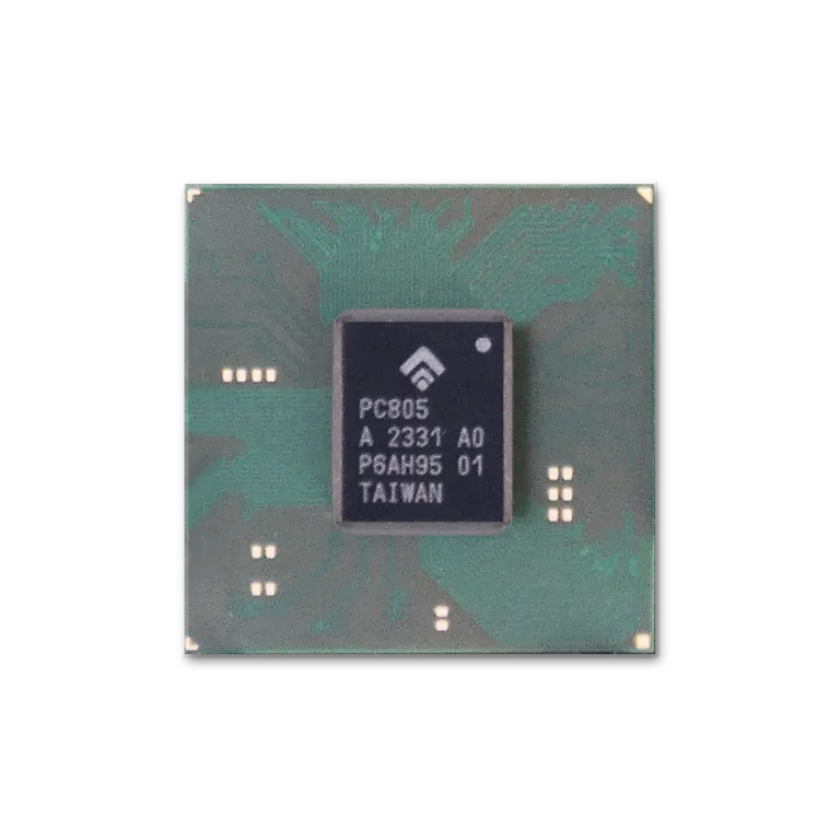
Picocom’s PC805 5G SoC delivers a small footprint and low power for 5G small cell O-RUs in enterprise, industrial, neutral host and private networks.

Picocom recently introduced the PC805, claiming the industry’s first system-on-chip (SoC) optimized for 5G small cell Open RAN radio units (O-RUs). The small footprint, low-power 5G O-RU SoC is designed to ease the implementation of 5G NR/LTE small cell O-RUs for use cases such as enterprise, industrial, neutral host, and private networks.

Simplifying the design of O-RUs, the PC805 PHY SoC meets Open RAN specifications and interfaces with an O-DU (as part of an Open RAN split 7.2) via an Open Fronthaul eCPRIi interface. It supports seamless connections to RFICs with a JESD204B high-speed serial interface.

An external processor/controller for configuration is not necessary. Configuration is performed via an integrated RISC-V based management processor running a Linux OS, Picocom said.

The PC805 performs aggregation of four or more 4T4R carriers at a 200-MHz instantaneous bandwidth (IBW) and is operational in U.S. CBRS and equivalent bands that are rapidly becoming available in other countries. A single PC805 supports multiple bands, including both TDD and FDD for 5G NR and LTE, with a cascade of two SoCs doubling the bandwidth supported.

The PC805 is available in a 17 × 17-mm FC LFBGA form factor. Samples will be available to lead customers, starting in November 2023. The PC805 launch includes a complete software suite and an RU demonstrator board (PC805RDB), which is a flexible 5G NR/LTE radio unit board used to demonstrate the PC805 SoC with an onboard RF transceiver, front-end and associated support circuitry, and software.

Picocom recently partnered with Texas Instruments on a 5G O-RAN outdoor RU reference design that leverages Picocom’s PC802 PHY SoC and TI’s AFE7769D transceiver.

The latest 32-bit RX MCU from Renesas features an integrated high-precision AFE and delivers 8× faster data rates than previous devices.

Renesas Electronics Corp. has expanded its 32-bit microcontroller (MCU) offering with a new RX MCU for high-end industrial sensor systems. The new RX23E-B 32-bit RX MCU features a high-precision analog front end (AFE), specifically designed for systems that require fast and accurate analog signal measurements.

The 32-bit RX MCU integrates a 24-bit Delta-Sigma A/D converter capable of achieving a conversion speed of up to 125 kSPS (125,000 samples/second), which is eight times faster than the existing RX23E-A, according to Renesas. It also can process accurate A/D conversion while reducing RMS noise to 1/3 (0.18 µVrms @1kSPS) when compared to the RX23E-A.

Delivering faster and more precise measurements of parameters such as strain, temperature, pressure, flow rate, current and voltage, the RX23E-B is suited for high-end sensor devices, measuring instruments and test equipment and can address a broad range of mid- to high-end system applications. For example, the RX23E-B offers sufficient performance to drive force sensors used in industrial robots, which often require measurements as fast as 10 µsec (100,000 samples/second), Renesas said. The MCU also reduces overall system size and the component count by integrating the AFE and the MCU on a single chip.

“In distributed processing designs, instead of relying on a dedicated MCU to manage all functions, each function can operate as a separate module, responsible for tasks such as motor control, sensor measurement and temperature control,” Renesas said.

Engineers can develop sensor modules more easily using an MCU with a built-in AFE than combining a discrete AFE chip and a separate MCU, in distributed processing designs such as large-scale instruments that control and take measurements of multiple targets like robot arms and gas and liquid analyzers, said the company.

Like the RX23E-A, the RX23E-B incorporates a 32-MHz RXv2-based CPU with digital signal processing (DSP) instructions and a floating point unit (FPU) and combines the AFE into a single chip using the same fabrication process. It offers new peripheral functions such as a 16-bit D/A converter, which enables measurement adjustments, self-diagnosis and analog signal output. Other features include an LCD controller with a maximum of 40 SEG × 4 COM and a real-time clock (RTC) function.

In addition, the RX23E-B’s +/-10-V analog input enables +/-10-V measurement with a 5-V power supply without requiring external components or additional power supply.

 The RX23E-B offers a version that supports an A/D conversion data rate of up to 125 kSPS, and one that supports up to 31.25 kSPS. Both products offer flexible data rate settings ranging from 3.8 SPS to the maximum value. This allows users to choose the best balance between data rate and noise for their specific system requirements, Renesas said.

The RX MCUs are available in a 5.5-mm2 100-pin BGA package and a 6-mm2 40-pin QFN package. They are also available in wide pin packages ranging from 48- to 100-pin options.

Both the RX23E-B and RX23E-B starter kit are available now. With the kit, engineers can evaluate the functionality of the AFE and signal conversion without the need for software development, Renesas said.

Renesas also offers the high-speed Pressure Control Solution Winning Combination design that combines the RX23E-B MCU with intelligent power devices that drive solenoid valves. The integrated high-precision AFE provides precise pressure control and minimizes the component count for the design, which reduces the BOM costs and board mounting area.

The NXP Trimension NCJ29D6 UWB IC family combines secure precise real-time localization and short-range radar, addressing multiple use cases with a single system.

NXP Semiconductors’ new Trimension NCJ29D6 is an automotive single-chip ultra-wideband (UWB) family that allows OEMs to use a single system for multiple use cases. The UWB IC family provides real-time secure car access and in-cabin sensing for child presence detection, seat belt reminder, intrusion alerts and kick sensor for automatic trunk opening as well as gesture recognition. The chips also reduce system cost and deliver greater system performance.

The new family is comprised of the highly integrated NCJ29D6B UWB device for secure car access, delivering enhanced ranging performance, reduced system costs, higher security and turn-key software, and the pin-to-pin compatible NCJ29D6A, claimed as the industry’s first automotive device that combines both ranging and short-range UWB radar in a single chip with an integrated MCU.

The multi-purpose platform enables OEMs to transform a single UWB-based car access system into a fully flexible platform that enables many use cases using the same hardware. OEMs can eliminate redundant systems and reduce cost, space and weight, NXP said, while additional features can be implemented through software updates, reducing total cost of ownership, while getting new features to market faster.

The NCJ29D6B features hands-free car access through a digital key on a UWB-enabled mobile phone. Delivering several performance enhancements, the device provides higher RF sensitivity and two simultaneous operating receiver chains that support antenna diversity and angle-of-arrival concepts that detect small changes in distance or direction of movement of other UWB-enabled devices. With a focus on system cost, it also features increased CPU performance, a larger memory size and high levels of integration, including an integrated digital CAN transceiver. Pin-to-pin compatibility extends the location features with short-range UWB radar.

Expectations are that cybersecurity and physical attacks will continue to increase. The new family enables integrated security capabilities that exceed the existing ISO21434 Cyber Security Requirements. CCC MAC and FiRa MAC offer standard compatible UWB ranging protocols that dock directly to the customer application software, enabling and simplifying AUTOSAR architectures, NXP said.

Automotive OEM and Tier 1 use cases are expected in model year 2025 vehicles. Evaluation and development boards for the Trimension NCJ29D6  include the TE Antenna Board for UWB Applications and Vivaldi Antenna for UWB Applications.