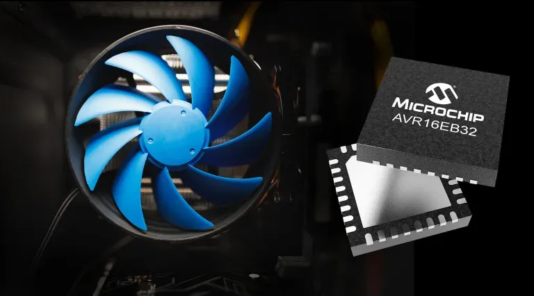
Microchip introduces the AVR EB family of MCUs that reduce noise, vibration and harshness in BLDC motors, while addressing efficiency and device longevity.


Microchip Technology Inc. has introduced its AVR EB family of microcontrollers (MCUs) that reduces noise, vibration and harshness (NVH) in brushless DC (BLDC) motors, while addressing efficiency and device longevity in a variety of cost-sensitive applications.

Microchip said historically cost-optimized controllers couldn’t deliver these benefits because they required sophisticated control algorithms and waveforms that were outside the capability of these controllers. The new AVR EB MCUs can adjust speed, timing and waveform shape—creating sinusoidal and trapezoidal waveforms—to improve the smoothness of motor operations, reduce noise and increase efficiency at high speeds.

In addition, these adjustments can be made on the fly, with near-zero latency, thanks to on-chip peripherals that enable multiple functions with minimal programming. Benefits include a reduction in code complexity, faster response to changes in operating conditions and lower overall bill of materials cost since several tasks, such as reading environmental sensors and serial communication, can be performed independent of the CPU, Microchip said.

Key features include a new 16-bit timer/counter E (TCE) with four compare channels for pulse-width modulation and waveform extension for BLDC motor control with tunable dead band insertion, a new 24-bit timer/counter F (TCF) for frequency generation and timing and a new programming and debug interface disable for advanced code security. In addition, the devices are housed in a small 3 mm × 3 mm package that can be mounted directly to the motor.

The AVR EB family is supported in Microchip’s MPLAB Development Ecosystem. A new Curiosity Nano Development Board is available for rapid prototyping. The AVR16EB32 Curiosity Nano Evaluation Kit (EV73J36A) connects to MPLAB X, Microchip Studio and IAR Embedded Workbench Integrated Development Environments (IDEs). The MPLAB Code Configurator (MCC) Melody graphical configuration tool also is available to accelerate design development.

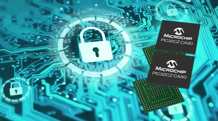
The Microchip PIC32CZ CA 32-bit MCUs with an embedded hardware security module make it easier to integrate security into industrial and consumer applications.

Microchip Technology Inc. offers a new family of PIC32CZ CA 32-bit microcontrollers (MCUs), providing designers with an easy path to integrate security functionality into their devices. The PIC32CZ CA 32-bit MCUs feature a 300-MHz Arm Cortex-M7 processor, an integrated hardware security module (HSM) and a wide range of connectivity and Flash memory options, targeting industrial and consumer applications.

The PIC32CZ CA devices include the PIC32CZ CA90 with an integrated HSM and the PIC32CZ CA80 without the integrated HSM. The HSM is a monolithic solution that provides advanced security, operating as a secure subsystem with a separate MCU on board. The MCU runs firmware and security features including hardware secure boot, key storage, cryptographic acceleration and true random number generator.

When additional security is necessary, factory provisioning is available on the PIC32CZ CA90 so that the devices are ready to be deployed. Microchip’s Trust Platform Development Suite, an in-house secure provisioning tool, enables a secure supply chain channel at scale or in low-volume production.

The PIC32CZ CA MCUs are configurable using such connectivity options as USART/UART, I2C, SPI, CAN FD, high-speed USB and Gigabit Ethernet. The Ethernet option includes Audio Video Bridging (AVB) and Precision Time Protocol (PTP) based on the IEEE 1588 standard. Users can expand functionality through Arduino Uno R3, Mikroe Bus or Xplained Pro compatible expansion boards. The devices are scalable with 2, 4 or 8 MB of on-board Flash, 1 MB of SRAM and error correction code (ECC) memory to mitigate data corruption.

Both devices are available now. The PIC32CZ CA80 is priced at $14.80 each and the PIC32CZ CA90 is available for $15.54 each, both in quantities of 10,000. The devices are supported by the PIC32CZ CA90 Curiosity Ultra Development Board, the PIC32CZ CA80 Curiosity Ultra Development Board and MPLAB Harmony v3 for testing, programming and debugging in the design phase.

Everspin introduces the EMxxLX STT-MRAM family with additional capacity options, smaller packaging and an extended temperature range.

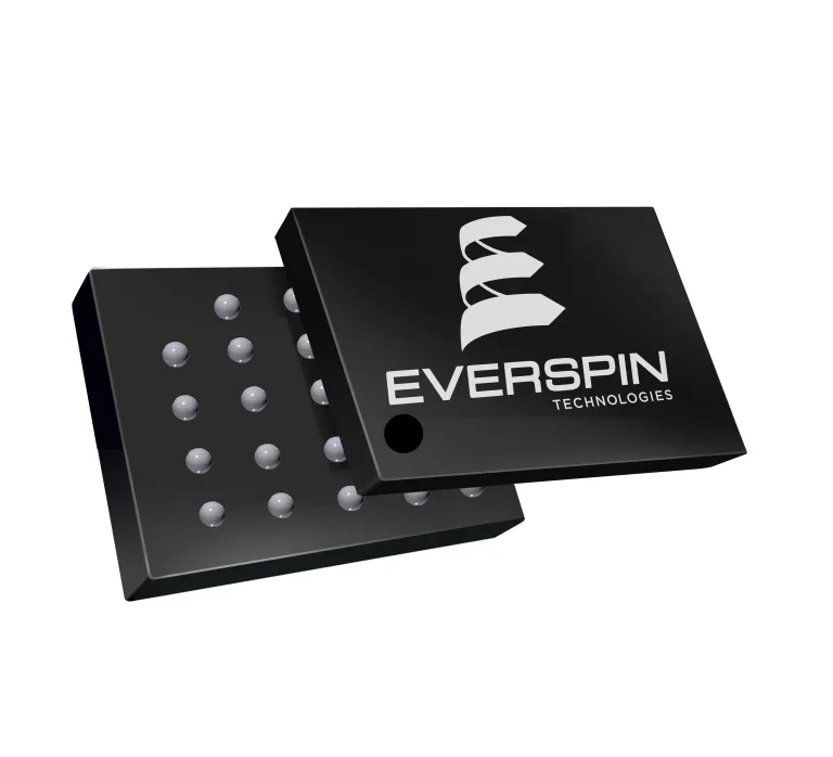
Everspin Technologies has expanded its flagship STT-MRAM product family with the introduction of the EMxxLX devices. This new family targets electronic systems where data persistence and integrity, low power, low latency and security are critical. The expansion adds a 4-Mbit capacity, a smaller package and an extended temperature range.

The EMxxLX offers enhanced performance, endurance and retention in densities from 4-to-64 megabits (Mbits) with new and smaller packaging for 4-to-16 Mbit devices. The new 5 × 6-mm DFN package reduces area by 37% compared to the previous footprint. The extended operating temperature ranges from -40°C to 105°C.

The family replaces solutions such as SRAM, BBSRAM, FRAM, NVSRAM and NOR flash devices. Applications include industrial IoT, network enterprise infrastructure, process automation and control, aeronautics/avionics, medical, gaming and FPGA configuration.

The STT-MRAM technology features high-performance, multiple I/O and a high-speed, low-pin-count SPI-compatible bus interface with a clock frequency of up to 200 MHz. The MRAM devices operate on a 1.8-V power supply and deliver a read/write bandwidth of 400 MB/s using eight I/O signals.

Expanding the MRAM’s capabilities results in protecting critical system data under any condition including power loss. The EMxxLX product line features SRAM-like performance, low latency and the capability to maintain memory without requiring power. By adding a 4-Mbit capacity, the MRAM devices increase the options for optimal density solutions, combined with ease of integration, said the company.

Everspin is now sampling the 4-Mbit capacity with the smaller DFN package, with production planned for the first quarter of 2024. Production orders of the 8-Mbit to 64-Mbit capacity options with the extended temperature range are available.

Nordic’s fourth generation Bluetooth LE SoC delivers higher performance and efficiency, expanded memory, new peripherals and advanced security.

Nordic Semiconductor has unveiled an addition to its nRF54 Series of Bluetooth Low Energy (LE) system-on-chip (SoCs) for the next generation of wireless IoT products in medical/healthcare, smart home, industrial IoT, VR/AR, PC accessories, remote controllers and gaming controller applications. The new nRF54L15 is the first Bluetooth LE SoC in the nRF54L Series, delivering increased processing power and efficiency, more memory and lower power consumption. The ultra-low-power Bluetooth 5.4 SoC also includes a new multiprotocol radio and advanced security features in a compact package.

The nRF54L15 SoC features an Arm Cortex-M33 processor running at 128 MHz, providing twice the processing power of the nRF52840 SoC while reducing power consumption. It is supported by 1.5 MB of non-volatile memory and 256 KB of RAM for concurrent running of multiple protocols.

The nRF54L15 SoC incorporates advanced hardware and software security designed for PSA Certified Level 3, the highest in the PSA Certified IoT security standard. Security features include secure boot, secure firmware update, secure storage, as well as protection against physical attacks thanks to integrated tamper sensors and cryptographic accelerators hardened against side-channel attacks.

The SoC’s new long-range multiprotocol radio provides up to 8-dBm TX power (with 1-dB increments) and -98-dBm RX sensitivity for 1 Mbits/s BLE. In addition, the radio features a new 4-Mbits/s data rate option for 2.4-GHz proprietary protocols, offering improved throughput, efficiency and latency, Nordic said. It supports all Bluetooth 5.4 features, Bluetooth Mesh and future Bluetooth spec updates as well as Thread and Matter.

Compared with the nRF52 series, the radio power consumption of the nRF54L15 offers significant improvements in TX and RX. For example, the radio RX current is cut in half, on a 1.8 VDC supply, delivering energy savings and allowing for smaller batteries or extended battery life.

Greater energy savings come from a new global real-time clock peripheral that can wake up the SoC from its deepest sleep mode, eliminating the need for an external RTC and reducing power consumption when applications sleep for long durations. Other new peripherals include a 14-bit ADC and a software-defined peripheral enabled by a RISC-V coprocessor.

The nRF54L15 is available to select customers for sampling. It is available in a 6 × 6-mm QFN package with 31 GPIOs, and in an ultra-compact 2.4 × 2.2-mm WLCSP with 32 GPIOs (300-µm pitch) and 14 GPIOs (350-µm pitch). These WLCSPs are more than 50 percent smaller than the nRF52840 WLCSP, making them suitable for designs with strict size constraints.

Infineon’s new TRAVEO T2G cluster family of automotive MCUs with a new graphics engine delivers new smart rendering technology.

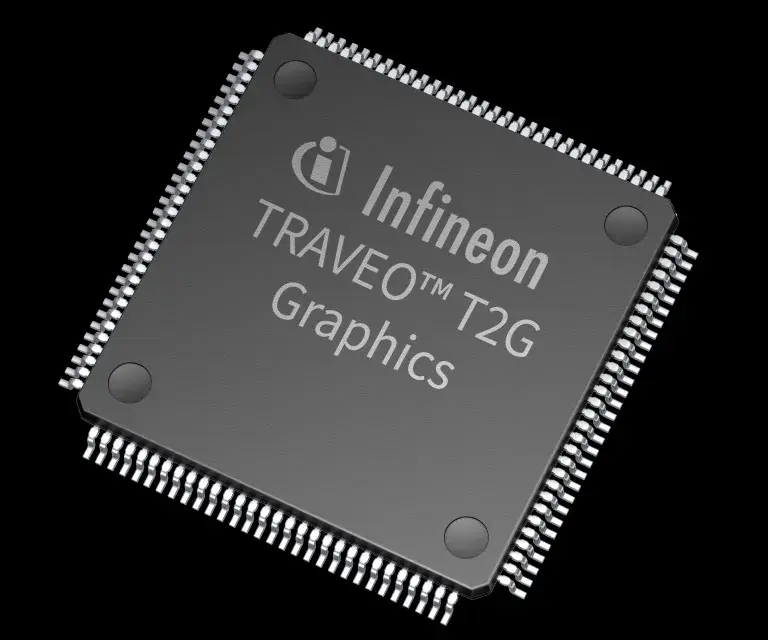
Infineon Technologies AG has unveiled its TRAVEO T2G cluster family of automotive microcontrollers (MCUs) with a new graphics engine, claiming outstanding performance for automotive graphics applications with a new smart rendering technology. The graphics engine minimizes the memory required for graphics processing by a factor of 3 to 5 for lower power consumption and lower costs.

The optimized 2.5 D graphics engine also enables the MCUs to support full virtual instrument clusters with a high resolution of up to 1920 × 1080, Infineon said.

With a dedicated graphics accelerator, the TRAVEO T2G cluster MCU family enables cluster, infotainment and cockpit systems with microprocessor performance at MCU cost, according to the company.

“The MCU family uses innovative line-based processing based on an Infineon patent, which enables significant line buffer savings by a factor of 10 compared to competitive devices, resulting in lower power consumption, less memory needs and lower BOM cost,” said Ralf Koedel, Infineon’s vice president for microcontroller smart mobility, in a statement.

The small footprint of the automotive MCUs also make them easier to integrate, while reducing BOM costs, said the company. This makes them suited for a variety of applications, including advanced smart mobility instrument cluster and heads-up display systems for automobiles, motorcycles, and off highway mobility as well as for industrial and medical applications.

Based on up to two Arm Cortex-M7 cores with up to 320 MHz, the TRAVEO T2G cluster microcontroller family enables ASIL-B/SIL-2 safety performance. The MCU family features up to 6 MB of Flash and up to 4 MB of internal VRAM or 1-GB LPPDR4 VRAM. Security features include an EVITA high-level HSM that provides advanced security with hardware encryption accelerators and enhanced hardware protection with a dedicated ARM Cortex-M0+.

The MCUs are available in a wide range of packages, ranging from 500-pin BGA (via 216-pin TEQFP) to 144-pin LQFP. CAN-FD, LIN, Gigabit Ethernet and CXPI are available as embedded peripherals. Other features include a JPEG decoder, video input and output and two serial memory interfaces (SPI or xSPI). HMI tools are available from partners to support key hardware features.

The TRAVEO T2G CYT2CL series (Arm Cortex-M4F core at 160 MHz, 4 MB of embedded flash), the TRAVEO T2G CYT3DL series (Arm Cortex-M7F core at 240 MHz, 4 MB of embedded flash and 2 MB VRAM) and the TRAVEO T2G CYT4DN series (Dual Arm Cortex-M7F core at 320 MHz, 6 MB of embedded flash and 4MB VRAM) are available and can be ordered now. Engineering samples of the TRAVEO T2G CYT4EN (Dual Arm Cortex-M7F core at 320 MHz, 6 MB of embedded flash, LPDDR4 and eMMC interface) are also available.

Ceva’s enhanced NeuPro-M NPU IP addresses generative AI workloads to support transformer networks, CNNs and other neural networks.

Transformer-based networks driving generative AI need a massive increase in compute and memory resources and optimized processing architectures. In response, Ceva has enhanced its NeuPro-M NPU IP family, addressing generative AI processing with high performance and power efficiency for AI inferencing workloads from the cloud to the edge.

The NeuPro-M NPU IP is designed for both classic AI and generative AI workloads. The architecture and tools were extensively redesigned to support transformer networks, CNNs and other neural networks and for future machine-learning inferencing models. This allows highly optimized applications that leverage generative and classic AI to be seamlessly developed and run on the NPU in communication gateways, optically-connected networks, cars, notebooks and tablets, AR/VR headsets and smartphones.

The power-efficient NeuPro-M scalable NPU architecture offers peak performance of 350 tera operations per second per watt (TOPS/W) at a 3-nm process node, Ceva said, and can process more than 1.5-million tokens per second/W for transformer-based LLM inferencing. It provides a full AI software stack that includes the NeuPro-M system architecture planner tool, neural network training optimizer tool and CDNN AI compiler and runtime.

The NeuPro-M meets stringent safety and quality compliance standards including automotive ISO 26262 ASIL-B functional safety standard and A-Spice quality assurance standards. The NPU architecture also supports secure access in the form of optional root of trust, authentication against IP/identity theft, secure boot and end-to-end data privacy.

The NeuPro-M architecture is flexible and future proof thanks to an integrated vector processing unit (VPU), supporting future network layers, said Ceva. The architecture also supports any activation and data flow, with true sparsity for data and weights that enables up to 4× acceleration in performance, the company added.

As a result, multiple applications and multiple markets can be addressed with a single NPU family. For larger scalability, the NeuPro-M adds the new NPM12 and NPM14 NPU cores, with two and four NeuPro-M engines, respectively, to migrate to higher performance AI workloads. The enhanced NeuPro-M family consists of four NPUs – the NPM11, NPM12, NPM14 and NPM18.

The enhanced NeuPro-M architecture also includes a revamped development tool chain, based on Ceva’s neural network CDNN AI compiler and CDNN software, architecturally aware for full utilization of NeuPro-M parallel processing engines and for maximizing AI application performance.

The NPM11 NPU IP is generally available with the NPM12, NPM14 and NPM18 available for lead customers.

Rohm’s BD5310xG-CZ/BD5410xG-CZ series delivers a class-leading withstand voltage and a wide operating voltage range.

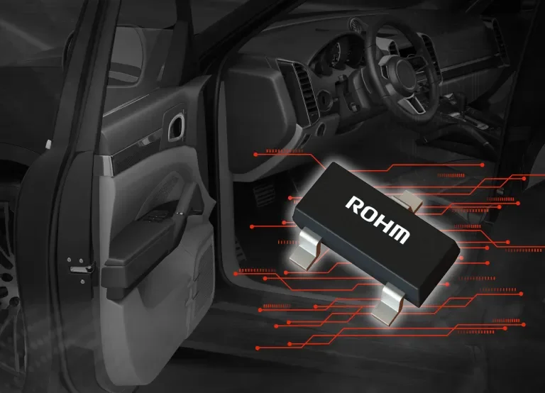
Addressing the need for increased electrification, functionality, comfort and safety in automotive applications, electronic control units (ECUs) and sensors are growing in number, especially Hall IC sensors. These Hall ICs deliver position detection and motor rotation on a non-contact basis so there is less wear than with mechanical switches. In response to the demand, Rohm Semiconductor has developed the BD5310xG-CZ/BD5410xG-CZ series for automotive applications.

Rohm said the new Hall-effect ICs provide an industry-leading 42-V withstand voltage for direct connection to a 12-V battery power supply. Target applications include automotive door locks, seat position, seat belts, wiper motors, power windows and sliding doors.

The BD5310xG-CZ offers unipolar detection required in door open/close and door locks, while the BD5410xG-CZ provides latch-type detection necessary for various motors including those used in power windows and sliding doors.

The series features a wide operating supply range of 2.7 V to 38 V and an internal topology that reduces power consumption by approximately 20 percent for a current consumption of 1.9 mA.

Both series comply with the AEC-Q100 (Grade 1) automotive reliability standard and provide the protection circuits required in vehicle systems. Eleven models are available in detection magnetic flux densities from 2.0 mT to 28.0 mT.

The Hall ICs are available now via Rohm’s distributors Digi-Key, Mouser and Farnell  and are scheduled for release at other online distributors.

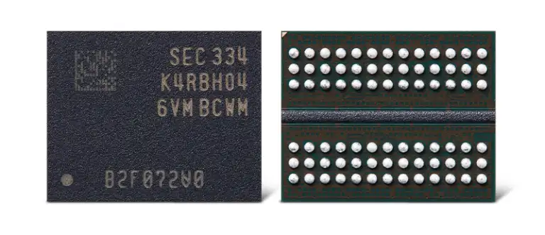
Samsung Electronics claims the first and highest-capacity 32-Gb DDR5 DRAM with 12-nm process technology for AI, data center and computing applications.

AI adoption often demands that greater performance be available across a myriad of industries and segments. This is also seen in the need for high-performance memory and data centers. To address these growing requirements, Samsung Electronics has claimed the industry’s first and highest-capacity 32-Gb DDR5 DRAM using 12-nanometer (nm) process technology.

The DRAM doubles the capacity of 16-Gb modules in a single chip, using the same package size, enabling the production of 128-GB DRAM modules while eliminating the through silicon via (TSV) process and decreasing power consumption by 10%.

Samsung explained that DDR5 128-GB DRAM modules using the 16-Gb DRAM required the TSV process. By moving to 32-Gb DRAM, the 128-GB module can be manufactured without this process, resulting in lower power consumption.

This latest announcement falls on the heels of Samsung announcing mass production of its 12-nm 16-Gb DDR5 DRAM in May 2023 that reduced power consumption by up to 23% while enhancing wafer productivity by up to 20%. Samsung’s 12-nm DDR5 DRAM lineup will support applications such as data centers, artificial intelligence (AI) and next-generation computing.

Now, Samsung claims that the 12-nm 32-Gb DRAM will enable DRAM modules of up to 1-terabyte (TB), providing the high-capacity DRAM necessary for AI and big data.

Mass production of the new 12-nm 32-Gb DDR5 DRAM is scheduled to begin by the end of 2023.

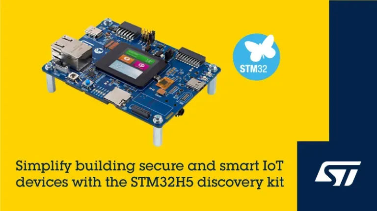
STMicroelectronics launched a Discovery Kit dev board to help designers explore the features of the STM32H5 MCUs for a range of applications.

STMicroelectronics has released a new development board that enables developers to explore a range of applications with the STM32H5 microcontrollers (MCUs). Applications include high-performance processing and advanced security in smart sensors, smart appliances, industrial controllers, networking equipment, personal electronics and medical devices.

The STM32H5 features the Arm Cortex-M33 embedded MCU core running at 250 MHz and is the first MCU to support ST’s Secure Manager turnkey system-on-chip security solutions. These include the Arm TrustZone security and ST’s STM32Trust framework to provide trusted storage, cryptography, attestation and updates, embedded with side-channel protected hardware cryptographic accelerators, targeting recognized security certifications, PSA Certified Level 3 and GlobalPlatform SESIP3.

With the STM32H573I-DK Discovery Kit, developers can evaluate the integrated features of the STM32H5 MCUs, such as analog peripherals, timers, the ST ART (Adaptive Real-Time) Accelerator, media interfaces and mathematical accelerators for new designs. Applications include industrial programmable logic controllers (PLC), motor drives and smart controllers for appliances such as air conditioners, refrigerators and washing machines. Other applications include alarm controllers, communication hubs and smart lighting controls.

The discovery kit includes an STM32H5 MCU, color touch display, digital microphone and interfaces such as USB, Ethernet and Wi-Fi. Other features include an audio codec, flash memory and headers for connecting expansion shields and daughterboards.

Also available is the STM32CubeH5 MCU software package that consolidates the components required to develop an application on the STM32H5, including examples and application code. The package is integrated into the STM32Cube ecosystem, which also provides additional software for application development. ST also offers the STM32CubeMX tool for configuring and initializing the MCU.

The Discovery Kit and the H5 Nucleo Board NUCLEO-H563ZI are now available from ST’s eStore and authorized distributors. The Discovery Kit board is priced at $98.75 and the Nucleo Board at $28.75.

Renesas customers can now share data between embedded and AI/ML projects for faster edge and endpoint AI application development in IoT networks.

Renesas Electronics Corp. has integrated its Reality AI Tools and e² studio integrated development environment (IDE) to simplify AIoT system development, allowing designers to seamlessly share data, projects and AI code modules between the programs. By creating these interfaces between embedded and AI/ML projects, designers will be able to experience faster design cycles for AI and TinyML applications at the edge and endpoint of IoT networks.

Modules for real-time data handling are now integrated in the Renesas MCU Software Development Kits. These include the Flexible Software Package (FSP) for RA, Firmware Integration Technology (FIT) for RX and Software Integration System (SIS) for RL78. This will facilitate data collection from Renesas kits or customer hardware using the MCUs.

Reality AI Tools allow engineers to generate and build TinyML/Edge AI models using advanced signal processing, automatically exploring sensor data and generating optimized models. The tools contain analytics that identify the best sensor or combination of sensors, locations for sensor placement and automatic generation of component specs. Fully explainable model functions in terms of time/frequency domains and optimized code for Arm Cortex M/A/R implementations is included. The e² studio Eclipse-based IDE for Renesas MCUs offers a range of extended functions, covering all development processes from the downloading of sample code to debugging.

Based on the new integration, sensor data collected from Renesas MCU development kits and visualized and labelled in e2 studio can be easily transferred to associated projects in Reality AI Tools. Users can download and integrate AI/ML classifiers generated in Reality AI Tools from within e2 studio.

With cross-platform project awareness between embedded and AI environments, users can synchronize and transfer lists of projects in e2 studio from Reality AI Tools, associate an ane2 studio project with a Reality AI Tools project, and create a new Reality AI Tools project from within e2 studio.

Further supporting AIoT system development, Renesas is also building a library of application examples and reference solutions, offering a proof-of-concept or blueprint for specific use cases, said the company. The Renesas AI application library currently features over 30 reference solutions for use-cases ranging across real-time analytics, vision and voice applications.