
BZV55-C6V2,135
NXP Semiconductors
The NXP Semiconductors BZV55-C6V2,135 is a Zener diode featuring a 6.2V breakdown voltage and 500mW power rating. It comes in an LLDS package.


| Distributor | Stock | Pricing | MOQ | PKG | Lead Time | Date Code | On Order Quantity | On Order Delivery | |
|---|---|---|---|---|---|---|---|---|---|
|
275 pcs
|
275 pcs | On Request | 1 | On Request | On Request | On Request | On Request | On Request | |
|
142 pcs
|
142 pcs | On Request | 1 | On Request | On Request | 12+ | On Request | On Request |
| Category | |
| Manufacturer Name | |
| AEC Qualified | |
| Automotive Grade | |
| Industrial Grade | |
| Medical Grade | |
| Military Grade |
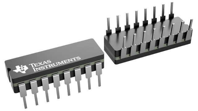
The Texas Instruments SN54LS75J is a 4-bit bistable latch, part of the LS technology family. It is designed for use as temporary storage for binary information between processing units and input/output or indicator units. Information present at a data (D) input is transferred to the Q output when the enable (C) is high and the Q output will follow the data input as long as the enable remains high. When the enable goes low, the information is retained at the Q output.
This latch features a maximum clock frequency of 35 MHz and operates within a temperature range of -55°C to 125°C, with a military rating. The input type is Bipolar and the output type is TTL. It has a maximum IOL of 8 mA and a maximum IOH of -0.4 mA, with a supply current of 46000 µA.
The SN54LS75J is available in a 16-CDIP package. All inputs are diode-clamped to minimize transmission-line effects and simplify system design. These circuits are completely compatible with all popular TTL families.
| Qty | Low | High |
|---|---|---|
| 1+ | $10.24 | $10.24 |
Estimated market price range - modelled values for guidance only, not live distributor offers.
The SN54LS75J operates over a temperature range of -55 to 125°C.
The maximum clock frequency for the SN54LS75J is 35 MHz.
The SN54LS75J has a TTL output type.
The SN54LS75J has 4 channels.
The SN54LS75J is available in a 16-CDIP package.

