| Distributor | Stock | Pricing | MOQ | PKG | Lead Time | Date Code | On Order Quantity | On Order Delivery | |
|---|---|---|---|---|---|---|---|---|---|
|
48 pcs
|
48 pcs | On Request | 1 | On Request | On Request | 1018 | On Request | On Request | |
|
1 pcs
|
1 pcs | On Request | 1 | On Request | On Request | On Request | On Request | On Request |
| Category | |
| Manufacturer Name | |
| Lead Spacing | |
| Mounting Type | |
| Number of I | |
| Number of LABs | |
| Number of Logic Elements | |
| Operating Temperature | |
| Supplier Device Package | |
| Total RAM Bits | |
| Voltage |
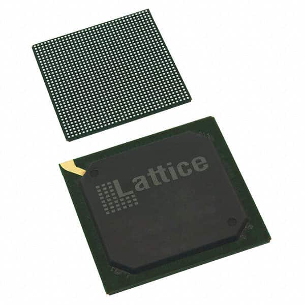
The Lattice Semiconductor Corporation LFE3-70EA-8FN1156C is a Field Programmable Gate Array (FPGA) designed for high logic density and system integration. It offers 67,000 logic elements and 8,375 logic array blocks, providing substantial capacity for complex designs.
This FPGA features 490 I/O pins and a total of 4.53 Mbits of RAM, including 4420 kbit of embedded block RAM and 145 kbit of distributed RAM. It operates within a voltage range of 1.14V to 1.26V, with a typical operating voltage of 1.2V, and can achieve a maximum operating frequency of 500 MHz.
The device is housed in a 1156-FPBGA (35x35) package and is designed for surface mount installation. It operates within a temperature range of 0°C to 85°C (TJ). The LFE3-70EA-8FN1156C is part of the ECP3 family and the LFE3 series, offering flexible configuration and robust performance for embedded applications.

The LFE3-70EA-8FN1156C FPGA has 67,000 logic elements.
The LFE3-70EA-8FN1156C FPGA has 490 I/O pins.
The operating voltage for the LFE3-70EA-8FN1156C FPGA is 1.2V.
The LFE3-70EA-8FN1156C FPGA is supplied in a 1156-FPBGA (35x35) package.
The maximum operating frequency of the LFE3-70EA-8FN1156C FPGA is 500 MHz.
The operating temperature range for the LFE3-70EA-8FN1156C FPGA is 0°C to 85°C (TJ).