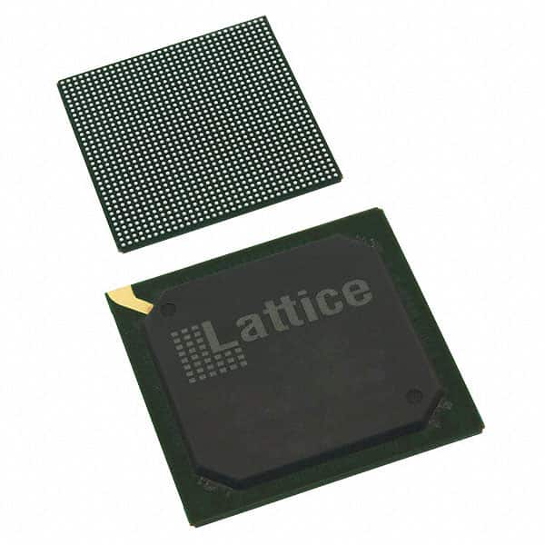
The Lattice LFE3-70EA-6FN1156C is a Field Programmable Gate Array (FPGA) belonging to the LatticeECP3 family. This device features a high logic density with 67,000 LUTs and 8,375 LABs, providing ample resources for complex designs. It offers 490 I/O pins for interfacing with other system components.
Key electrical characteristics include an operating voltage range of 1.14V to 1.26V, with a nominal 1.2V core supply. The FPGA is equipped with flexible memory resources, including up to 6.85 Mbits of embedded Block RAM and 303K bits of distributed RAM, totaling 4.53 Mbits of on-chip memory. It also supports embedded SERDES functionality with data rates up to 3.2 Gbps per channel, enabling high-speed serial communication.
The device operates within a temperature range of 0°C to 85°C (TJ) and is housed in a 1156-FPBGA package, designed for surface mounting. The LatticeECP3 family is known for its balance of performance, power efficiency, and cost-effectiveness, making it suitable for high-volume applications.