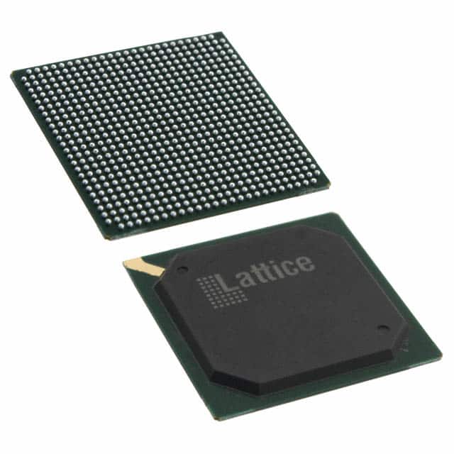
The Lattice LFE2M50E-6FN672I is a Field Programmable Gate Array (FPGA) from the LatticeECP2/M family. It offers a high logic density with 48,000 LUTs and 6,000 LABs, providing significant capacity for complex designs.
This FPGA features 372 I/O pins and a substantial 4,246,528 total RAM bits, enabling extensive memory resources. It operates within a voltage range of 1.14V to 1.26V and has an operating temperature range of -40°C to 100°C (TJ).
The device supports embedded SERDES with data rates up to 3.125 Gbps across up to 16 channels. It includes sysDSP blocks for high-performance multiply and accumulate operations, and flexible sysMEM embedded block RAM resources. The programmable sysI/O buffer supports a wide array of interfaces, including LVTTL, LVCMOS, SSTL, HSTL, LVDS, and LVPECL.
Packaged in a 672-FPBGA (27x27 mm) with surface mount mounting type, the LFE2M50E-6FN672I is designed for system integration and high-performance applications. It is also compliant with 1149.1 Boundary Scan standards and features an SPI boot flash interface.