| Distributor | Stock | Pricing | MOQ | PKG | Lead Time | Date Code | On Order Quantity | On Order Delivery | |
|---|---|---|---|---|---|---|---|---|---|
|
1,718 pcs
|
1718 pcs | On Request | 1 | On Request | On Request | On Request | On Request | On Request |
| Category | |
| Manufacturer Name | |
| Lead Spacing | |
| Mounting Type | |
| Number of I | |
| Number of LABs | |
| Number of Logic Elements | |
| Operating Temperature | |
| Supplier Device Package | |
| Total RAM Bits | |
| Voltage |
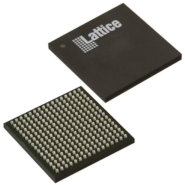
The Lattice Semiconductor LCMXO2-7000HC-6BG256I is a Field Programmable Gate Array (FPGA) from the MachXO2 family. It offers a flexible logic architecture with 6864 LUTs (Look-Up Tables) and 858 LABs (Logic Array Blocks), providing 206 I/O pins for interfacing.
This device features 245760 total RAM bits and 256 kbits of on-chip user flash memory with 100,000 write cycles. It operates within a voltage range of 2.375V to 3.465V and has an operating temperature range of -40°C to 100°C (TJ).
The LCMXO2-7000HC-6BG256I is supplied in a 256-CABGA (14x14) package and supports surface mount installation. It is designed for ultra-low power consumption, with standby power as low as 22 µW.
Key features include pre-engineered source synchronous I/O, flexible on-chip clocking with up to two analog PLLs, and non-volatile, infinitely reconfigurable architecture with instant-on capability. The device supports various I/O standards including LVCMOS, LVDS, and HSTL.

The LCMXO2-7000HC-6BG256I has 6864 logic elements.
The LCMXO2-7000HC-6BG256I offers 206 I/O pins.
The operating voltage range for the LCMXO2-7000HC-6BG256I is 2.375V to 3.465V.
The LCMXO2-7000HC-6BG256I is supplied in a 256-CABGA (14x14) package and a 256-LFBGA package.
The operating temperature range for the LCMXO2-7000HC-6BG256I is -40°C to 100°C (TJ).
The MachXO2 FPGA has a standby power consumption as low as 22 µW.
The LCMXO2-7000HC-6BG256I has up to 256 kbits of user flash memory.