

| Distributor | Stock | Pricing | MOQ | PKG | Lead Time | Date Code | On Order Quantity | On Order Delivery | |
|---|---|---|---|---|---|---|---|---|---|
|
114 pcs
|
114 pcs | On Request | 1 | On Request | On Request | 16+ | On Request | On Request |
| Category | |
| Manufacturer Name | |
| Lead Spacing | |
| Mounting Type | |
| Number of I | |
| Number of LABs | |
| Number of Logic Elements | |
| Operating Temperature | |
| Storage Temperature | |
| Supplier Device Package | |
| Supplier Package | |
| Tape & Reel | |
| Total RAM Bits | |
| Voltage |
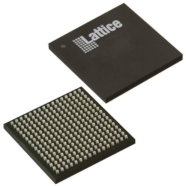
The Lattice Semiconductor LCMXO2-7000HC-5BG256I is an FPGA from the MachXO2 family, designed for flexible logic implementation. It offers 6864 logic elements and 858 LABs, providing substantial capacity for complex designs. The device supports up to 206 I/O pins and includes 245760 bits of embedded RAM.
This FPGA operates within a voltage range of 2.375V to 3.465V and has an operating temperature range of -40°C to 100°C (TJ). It is housed in a 256-LFBGA package, with a supplier package designation of 256-CABGA (14x14). The mounting type is Surface Mount.
The MachXO2 family is known for its ultra-low power consumption, advanced 65 nm process, and features like on-chip flash memory, pre-engineered source synchronous I/O, and flexible clocking. These FPGAs are non-volatile and infinitely reconfigurable, offering instant-on capabilities and secure, single-chip solutions.
This specific part, LCMXO2-7000HC-5BG256I, is suitable for applications requiring a balance of logic density, I/O count, and power efficiency. Its surface-mount package and operating temperature range make it adaptable for various embedded systems.
The LCMXO2-7000HC-5BG256I has 6864 logic elements.
This FPGA has a total of 245760 RAM bits.
There are 206 I/O pins available on this device.
The operating voltage range is 2.375V to 3.465V.
It is a 256-LFBGA package designed for surface mounting.
The operating temperature range is -40°C to 100°C (TJ).