

| Distributor | Stock | Pricing | MOQ | PKG | Lead Time | Date Code | On Order Quantity | On Order Delivery | |
|---|---|---|---|---|---|---|---|---|---|
|
46,020 pcs
|
46020 pcs | On Request | 1 | On Request | On Request | On Request | On Request | On Request |
| Category | |
| Manufacturer Name | |
| Lead Style | |
| Logic Type | |
| Mounting Type | |
| Number of Bits | |
| Operating Temperature | |
| Storage Temperature | |
| Supplier Device Package | |
| Supplier Package | |
| Supply Current | |
| Supply Voltage |
The HEF4007UBT,653 from NXP Semiconductors is a versatile integrated circuit featuring a dual complementary pair and inverter configuration. It is designed for a wide supply voltage range, from 3.0 V to 15.0 V, with absolute maximum ratings extending up to 18 V. The device offers high noise immunity and low CMOS power dissipation, making it suitable for various applications.
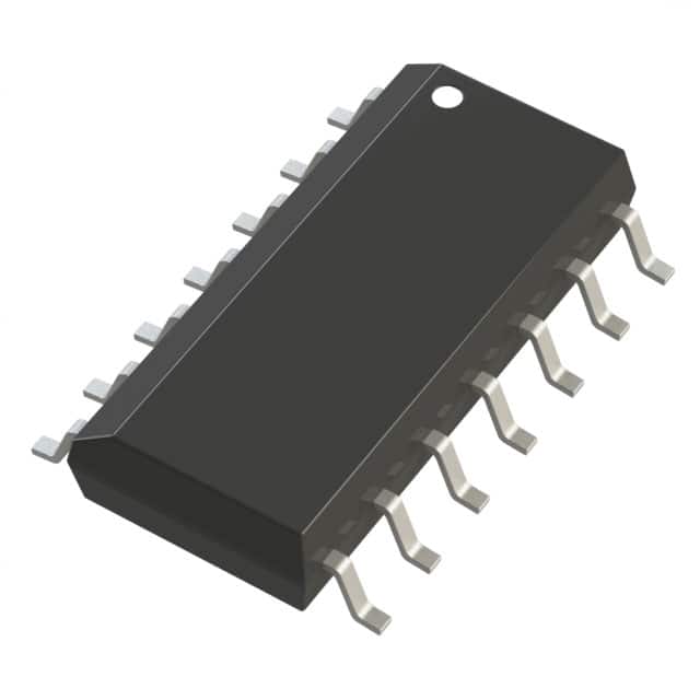
This IC operates within an ambient temperature range of -40 °C to +85 °C, with storage temperatures from -65 °C to +150 °C. It includes ESD protection exceeding 2000 V for HBM class 2 and 1000 V for CDM class C3. The HEF4007UBT,653 is supplied in a 14-lead SOIC package with a body width of 3.9 mm, suitable for surface mounting.
Key electrical characteristics include input clamping current of ±10 mA and output clamping current of ±10 mA. The total power dissipation is rated at 500 mW at 85 °C, with power dissipation per output at 100 mW. Inputs include clamp diodes, allowing the use of current-limiting resistors for interfacing with voltages exceeding VDD.
| Qty | Low | High |
|---|---|---|
| 1+ | $0.50 | $0.50 |
Estimated market price range - modelled values for guidance only, not live distributor offers.
The supply voltage range is 3.0V to 15.0V.
It comes in a 14-SOIC (0.154", 3.90mm Width) surface-mount package.
The operating temperature range is -40°C to +85°C.
The logic type is Complementary Pair Plus Inverter with 3 bits.
The maximum total power dissipation is 500mW, with 100mW per output.