

| Distributor | Stock | Pricing | MOQ | PKG | Lead Time | Date Code | On Order Quantity | On Order Delivery | |
|---|---|---|---|---|---|---|---|---|---|
|
25,020 pcs
|
25020 pcs | On Request | 1 | On Request | On Request | On Request | On Request | On Request |
| Category | |
| Manufacturer Name | |
| Configuration | |
| Current | |
| Drain to Source Voltage (Vdss) | |
| FET Feature | |
| Gate Charge (Qg) (Max) @ Vgs | |
| Input Capacitance (Ciss) (Max) @ Vds | |
| Mounting Type | |
| Number of Pins | |
| Operating Temperature | |
| Pitch | |
| Power | |
| Rds On (Max) @ Id, Vgs | |
| Storage Temperature | |
| Supplier Device Package | |
| Tape & Reel | |
| Technology | |
| Vgs(th) (Max) @ Id |
The BSS84AKV is a dual P-channel enhancement mode Field-Effect Transistor (FET) manufactured by Nexperia using Trench MOSFET technology. It is designed for logic-level gate operation and offers very fast switching capabilities.
Each transistor features a maximum drain-source voltage of -50V, continuous drain current of -170mA (at VGS = -10V, Tamb = 25°C), and peak drain current of up to 0.7A for single pulses. The drain-source on-state resistance is typically 4.5Ω with a maximum of 7.5Ω at VGS = -10V and ID = -100mA. The gate threshold voltage is maximum 2.1V at ID = 250µA. The device includes ESD protection up to 1kV (Human Body Model).
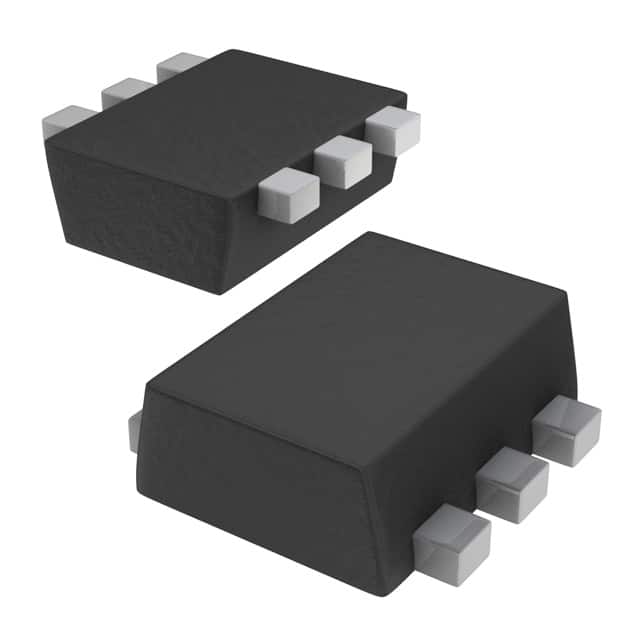
The device is housed in an ultra-small SOT-666 surface-mount package with 6 leads, 0.5mm pitch, and body dimensions of 1.6mm x 1.2mm x 0.55mm. Maximum power dissipation per device is 500mW at Tamb = 25°C, with 330mW per transistor. Operating junction temperature ranges from -55°C to 150°C.
Typical applications include relay drivers, high-speed line drivers, high-side load switches, and general switching circuits. The dual P-channel configuration makes it suitable for compact power management designs requiring matched transistors.
| Qty | Low | High |
|---|---|---|
| 1+ | $0.41 | $0.41 |
| 10+ | $0.25 | $0.25 |
| 100+ | $0.16 | $0.16 |
| 500+ | $0.12 | $0.12 |
| 1,000+ | $0.10 | $0.10 |
| 2,000+ | $0.09 | $0.09 |
| 4,000+ | $0.08 | $0.08 |
| 8,000+ | $0.07 | $0.07 |
| 24,000+ | $0.06 | $0.06 |
Estimated market price range - modelled values for guidance only, not live distributor offers.
The maximum drain-source voltage (VDS) is -50V.
The device is available in SOT-666 (also SOT-563) surface-mount package.
The operating junction temperature range is -55°C to 150°C.
The RoHS status is listed as RoHS3 Compliant, but this information is unverified.
The gate-source voltage (VGS) is rated from -20V to 20V at Tj = 25°C.
The continuous drain current (ID) is -170mA at VGS = -10V and Tamb = 25°C.
The drain-source on-state resistance (RDSon) is typically 4.5Ω, maximum 7.5Ω at VGS = -10V and ID = -100mA.