

| Distributor | Stock | Pricing | MOQ | PKG | Lead Time | Date Code | On Order Quantity | On Order Delivery | |
|---|---|---|---|---|---|---|---|---|---|
|
67,020 pcs
|
67020 pcs | On Request | 1 | On Request | On Request | On Request | On Request | On Request | |
|
205 pcs
|
205 pcs | On Request | 1 | On Request | On Request | On Request | On Request | On Request |
| Category | |
| Manufacturer Name | |
| AEC Qualified | |
| Automotive Grade | |
| Configuration | |
| Current | |
| Drain to Source Voltage (Vdss) | |
| ESD Protection | |
| FET Feature | |
| Gate Charge (Qg) (Max) @ Vgs | |
| Input Capacitance (Ciss) (Max) @ Vds | |
| Mounting Type | |
| Operating Temperature | |
| Power | |
| Rds On (Max) @ Id, Vgs | |
| Storage Temperature | |
| Supplier Device Package | |
| Tape & Reel | |
| Technology | |
| Vgs(th) (Max) @ Id |
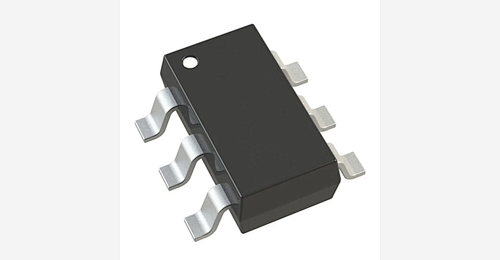
The BSS84AKS,115 is a dual P-channel enhancement mode MOSFET from Nexperia, fabricated using Trench MOSFET technology. It is designed for low-power switching applications and is AEC-Q101 qualified for automotive use. The device integrates two independent P-channel MOSFETs in a compact 6-TSSOP (SOT363) surface-mount package.
Key electrical specifications include a drain-source voltage rating of 50 V, continuous drain current of 160 mA per transistor (640 mA peak), and a maximum on-state resistance of 7.5 Ω at VGS = -10 V. The logic-level gate threshold voltage (max 2.1 V) allows direct drive from low-voltage logic. The device also features built-in ESD protection up to 1 kV (HBM).
With a typical gate charge of only 0.35 nC and input capacitance of 36 pF, the BSS84AKS offers very fast switching performance. Power dissipation is rated at 445 mW for the entire package (280 mW per transistor) at 25°C ambient. The operating junction temperature range is -55°C to 150°C.
Typical applications include relay drivers, high-speed line drivers, high-side load switches, and general switching circuits. The small footprint and dual-channel configuration make it ideal for space-constrained designs requiring independent P-channel switches.
| Qty | Low | High |
|---|---|---|
| 1+ | $0.38 | $0.38 |
| 10+ | $0.25 | $0.25 |
| 100+ | $0.16 | $0.16 |
| 500+ | $0.11 | $0.11 |
| 1,000+ | $0.10 | $0.10 |
| 3,000+ | $0.07 | $0.07 |
Estimated market price range - modelled values for guidance only, not live distributor offers.
The operating junction temperature range is -55°C to 150°C.
It is available in a 6-TSSOP (SOT363) surface-mount package.
The part is listed as RoHS3 Compliant, but this is unverified from the datasheet.
The maximum continuous drain current is 160 mA per transistor at 25°C ambient.
The maximum gate threshold voltage is 2.1 V at ID=250 µA.
Yes, it features ESD protection up to 1 kV (HBM).
Yes, it is AEC-Q101 qualified.