

| Distributor | Stock | Pricing | MOQ | PKG | Lead Time | Date Code | On Order Quantity | On Order Delivery | |
|---|---|---|---|---|---|---|---|---|---|
|
21,020 pcs
|
21020 pcs | On Request | 1 | On Request | On Request | On Request | On Request | On Request |
| Category | |
| Manufacturer Name | |
| Ambient Temperature | |
| Junction Temperature | |
| Lead Spacing | |
| Lead Style | |
| Mounting Type | |
| Storage Temperature | |
| Tape & Reel |
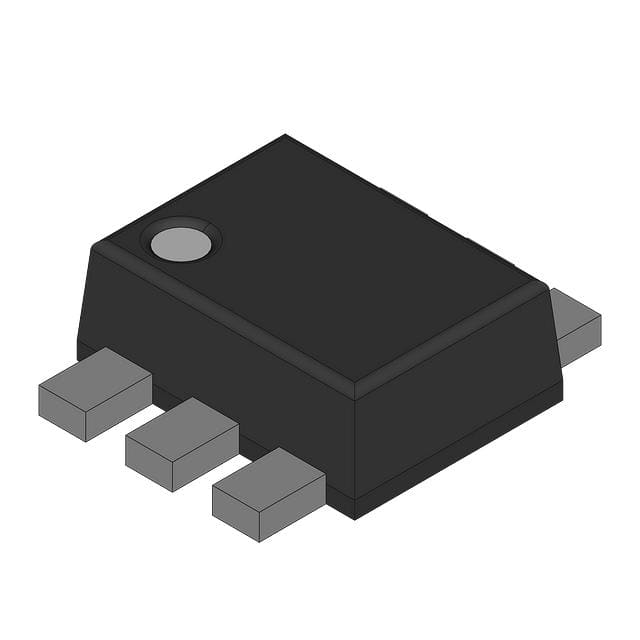
The Nexperia BC847BV115 is an NPN general purpose double transistor designed for switching and amplification applications. It is housed in an ultra-small SOT666 flat lead plastic package, measuring 1.6 mm x 1.2 mm x 0.55 mm, which helps reduce board space and pick-and-place costs.
Key electrical characteristics include a collector-emitter voltage (VCEO) of 45V and a collector current (IC) of up to 100mA per transistor. The DC current gain (hFE) ranges from 200 to 450 under typical test conditions (VCE = 5V, IC = 2mA, Tamb = 25°C).
This transistor offers improved thermal behavior due to its flat leads and excellent coplanarity. The total power dissipation per device is rated at 300 mW at an ambient temperature of 25°C. The operating and storage temperatures range from -65°C to 150°C.
Its compact size and performance make it suitable for general-purpose switching and amplification tasks where space is a constraint.
| Qty | Low | High |
|---|---|---|
| 1+ | $0.75 | $0.75 |
Estimated market price range - modelled values for guidance only, not live distributor offers.
The collector-emitter voltage (VCEO) for the BC847BV115 is 45V.
The maximum collector current (IC) for the BC847BV115 is 100mA.
The DC current gain (hFE) of the BC847BV115 is between 200 and 450.
The BC847BV115 is in a SOT666 package.
The SOT666 package for the BC847BV115 has body dimensions of 1.6 mm x 1.2 mm x 0.55 mm.
The total power dissipation (Ptot) for the BC847BV115 is 300mW per device at 25°C ambient.