Ready to onboard?
Are you ready to join DistyParts and
grow your business?


| Distributor | Stock | Pricing | MOQ | PKG | Lead Time | Date Code | On Order Quantity | On Order Delivery | |
|---|---|---|---|---|---|---|---|---|---|
|
11,020 pcs
|
11020 pcs | On Request | 1 | On Request | On Request | On Request | On Request | On Request |
| Category | |
| Manufacturer Name | |
| AEC Qualified | |
| AEC-Q101 | |
| Ambient Temperature (Minimum/Maximum) | |
| Automotive Grade | |
| Body Dimensions | |
| Capacitance @ Vr, F | |
| Current | |
| Junction Temperature | |
| Lead Spacing | |
| Lead Style | |
| Mounting Type | |
| Non Repetitive Peak Forward Current (Maximum @ tp = 1 µs, Tj(init) = 25 °C) | |
| Non Repetitive Peak Forward Current (Maximum @ tp = 10 ms, Tj(init) = 25 °C) | |
| Non Repetitive Peak Forward Current (Maximum @ tp = 100 µs, Tj(init) = 25 °C) | |
| Operating Temperature | |
| Package Description | |
| Package Name | |
| Repetitive Peak Forward Current | |
| Repetitive Peak Reverse Voltage | |
| Reverse Current @ VR | |
| Reverse Recovery Time (trr) | |
| Reverse Voltage | |
| SVHC Present | |
| Speed | |
| Storage Temperature | |
| Storage Temperature (Minimum/Maximum) | |
| Supplier Device Package | |
| Technology | |
| Termination Style | |
| Thermal Resistance Junction-to-Ambient | |
| Total Power Dissipation (Maximum @ Tamb ≤ 25 °C, FR 4 1 cm² cathode pad) | |
| Total Power Dissipation (Maximum @ Tamb ≤ 25 °C, FR 4 standard footprint) | |
| Voltage |
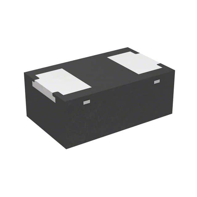
The BAS21LLYL is a high-voltage switching diode designed for fast switching applications. It is encapsulated in a leadless ultra small DFN1006-2 (SOD882) surface-mount plastic package. Key electrical characteristics include a maximum reverse voltage of 200V, repetitive peak reverse voltage of 250V, and a forward current of 330mA. The diode offers a fast reverse recovery time of 50ns, low leakage current of 100nA, and low capacitance of 2pF, making it suitable for high-speed switching and voltage clamping. The device is AEC-Q101 qualified for automotive applications. It is designed for general-purpose switching, reverse polarity protection, and voltage clamping. The package dimensions are 1mm x 0.6mm x 0.48mm with a 0.65mm lead spacing, suitable for compact PCB designs. The operating temperature range is -55°C to 150°C, with a maximum junction temperature of 150°C.
| Qty | Low | High |
|---|---|---|
| 1+ | $0.20 | $0.20 |
| 10+ | $0.12 | $0.12 |
| 50+ | $0.09 | $0.09 |
| 100+ | $0.07 | $0.07 |
| 500+ | $0.05 | $0.05 |
| 10,000+ | $0.03 | $0.03 |
| 30,000+ | $0.03 | $0.03 |
Estimated market price range - modelled values for guidance only, not live distributor offers.
The maximum reverse voltage is 200V, with a repetitive peak reverse voltage of 250V.
The maximum forward current is 330mA.
The forward voltage is typically 1.25V at 200mA forward current.
The reverse recovery time is 50ns.
It is available in a leadless DFN1006-2 (SOD882) surface-mount package with dimensions 1mm x 0.6mm x 0.48mm.
Yes, it is AEC-Q101 qualified.
The capacitance is 2pF at 0V and 1MHz.