

| Distributor | Stock | Pricing | MOQ | PKG | Lead Time | Date Code | On Order Quantity | On Order Delivery | |
|---|---|---|---|---|---|---|---|---|---|
|
8 pcs
|
8 pcs | On Request | 1 | On Request | On Request | On Request | On Request | On Request |
| Category | |
| Manufacturer Name | |
| Bandwidth | |
| Channel Capacitance (CS(off), CD(off)) | |
| Charge Injection | |
| Crosstalk | |
| Current | |
| Mounting Type | |
| Multiplexer | |
| Number of Circuits | |
| On | |
| Operating Temperature | |
| Supplier Device Package | |
| Switch Circuit | |
| Switch Time (Ton, Toff) (Max) | |
| Voltage |
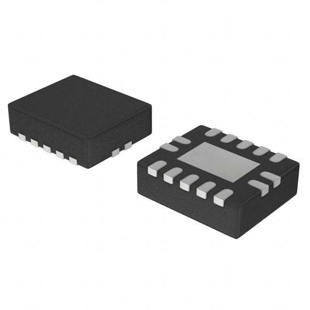
The 74LVC4066BQ,115 from Nexperia is a high-speed Si-gate CMOS device providing four single-pole, single-throw (SPST) analog switch functions. Each switch includes two input/output terminals (nY and nZ) and an active HIGH enable input (nE). When the enable input is LOW, the analog switch is turned off.
This device features a wide supply voltage range from 1.65 V to 5.5 V, making it versatile for various applications. It boasts very low ON resistance, typically 7.5 Ω at VCC = 2.7 V, 6.5 Ω at VCC = 3.3 V, and 6 Ω at VCC = 5 V. The switch current capability is 32 mA, and it offers high noise immunity with CMOS low-power consumption. Schmitt-trigger action at the enable inputs ensures tolerance to slower input rise and fall times across the entire VCC range. The part is available in a 14-DHVQFN (2.5x3) package and operates over a temperature range of -40°C to 125°C.
The 74LVC4066BQ,115 operates with a supply voltage range from 1.65V to 5.5V.
The 74LVC4066BQ,115 is supplied in a 14-VFQFN Exposed Pad package, specifically a 14-DHVQFN (2.5x3) supplier device package.
The 74LVC4066BQ,115 has an operating temperature range of -40°C to 125°C (TA).
The 74LVC4066BQ,115 is RoHS3 Compliant.
The typical ON resistance is 7.5 Ω at VCC = 2.7 V, 6.5 Ω at VCC = 3.3 V, and 6 Ω at VCC = 5 V.
The 74LVC4066BQ,115 has 4 circuits.
The switch current capability of the 74LVC4066BQ,115 is 32 mA.