5962-9682201QDA
Texas Instruments
The Texas Instruments 5962-9682201QDA is a MILITARY 4-CH, 2-INPUT, 2-V TO 5 current regulation transistor. It features a W CFP package with 14 pins.


| Distributor | Stock | Pricing | MOQ | PKG | Lead Time | Date Code | On Order Quantity | On Order Delivery | |
|---|---|---|---|---|---|---|---|---|---|
|
631 pcs
|
631 pcs | On Request | 1 | On Request | On Request | On Request | On Request | On Request |
| Category | |
| Manufacturer Name | |
| Mounting Type | |
| Storage Temperature | |
| Tape & Reel |
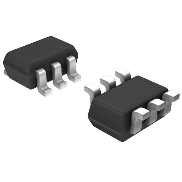
The 74LVC2G17GW,125 from NXP Semiconductors is a dual non-inverting buffer featuring Schmitt-trigger inputs. This device is designed for versatility, allowing inputs to be driven by either 3.3 V or 5 V devices, making it suitable for mixed-voltage environments.
Key electrical characteristics include a wide supply voltage range from 1.65 V to 5.5 V and overvoltage tolerant inputs up to 5.5 V. It provides ±24 mA output drive at 3.0 V and exhibits high noise immunity. The device also features IOFF circuitry for partial power-down operation and latch-up performance exceeding 250 mA.
This buffer is specified for operation across a broad temperature range of -40 °C to +125 °C. It is available in a 6-lead TSSOP package, suitable for surface mounting.
Applications include wave and pulse shaping in noisy environments, and direct interfacing with TTL levels.
| Qty | Low | High |
|---|---|---|
| 1+ | $0.30 | $0.30 |
Estimated market price range - modelled values for guidance only, not live distributor offers.
The operating voltage range is from 1.65 V to 5.5 V.
The operating temperature range is -40 °C to +125 °C.
It is supplied in a 6-lead TSSOP package.
The output drive is ±24 mA at VCC = 3.0 V.
Yes, the inputs are overvoltage tolerant to 5.5 V.