

| Distributor | Stock | Pricing | MOQ | PKG | Lead Time | Date Code | On Order Quantity | On Order Delivery | |
|---|---|---|---|---|---|---|---|---|---|
|
16,020 pcs
|
16020 pcs | On Request | 1 | On Request | On Request | On Request | On Request | On Request |
| Category | |
| Manufacturer Name | |
| AEC Qualified | |
| Automotive Grade | |
| Clock Frequency | |
| Current | |
| Function | |
| Input Capacitance | |
| Latch-up Performance | |
| Logic Type | |
| Max Propagation Delay @ V, Max CL | |
| Mounting Type | |
| Number of Bits per Element | |
| Number of Circuits | |
| Number of Elements | |
| Operating Temperature | |
| Output Type | |
| Supplier Device Package | |
| Supplier Package | |
| Trigger Type | |
| Type | |
| Voltage |
The Nexperia 74LVC1G175GV-Q100H is a single positive edge-triggered D-type flip-flop with an asynchronous active LOW master reset. It is designed for low-power, low-voltage applications and can interface directly with TTL levels.
Key electrical specifications include a wide supply voltage range from 1.65 V to 5.5 V, a maximum propagation delay of 4 ns at 5V/50pF, and a clock frequency of up to 200 MHz. The device offers ±24 mA output drive at 3.0 V and has an input capacitance of 2.5 pF. It also features Schmitt trigger action on all inputs for tolerance to slower input rise and fall times.
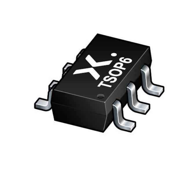
This flip-flop is specified for operation between -40 °C and +125 °C, making it suitable for demanding environments. It is available in a compact 6-TSOP (SC-74, SOT-457) surface-mount package, supplied on a reel.
The 74LVC1G175GV-Q100H is qualified to AEC-Q100 (Grade 1) standards, indicating its suitability for automotive applications. It also includes IOFF circuitry for partial power-down mode operation.
| Qty | Low | High |
|---|---|---|
| 1+ | $1.23 | $1.23 |
Estimated market price range - modelled values for guidance only, not live distributor offers.
The operating voltage range is 1.65 V to 5.5 V.
The operating temperature range is -40 °C to +125 °C.
It comes in a 6-TSOP package (SC-74, SOT-457) for surface mount.
The maximum clock frequency is 200 MHz.
The maximum propagation delay is 4 ns at 5V and 50pF load.
The typical output drive is ±24 mA at VCC = 3.0 V.
It exceeds 2000 V HBM (class 2) and 1000 V CDM (class C3).