

| Distributor | Stock | Pricing | MOQ | PKG | Lead Time | Date Code | On Order Quantity | On Order Delivery | |
|---|---|---|---|---|---|---|---|---|---|
|
10,000 pcs
|
10000 pcs | On Request | 1 | On Request | On Request | On Request | On Request | On Request |
| Category | |
| Manufacturer Name | |
| Current | |
| Input Capacitance | |
| Input Logic Level | |
| Input Voltage | |
| Latch-up Performance | |
| Logic Type | |
| Max Propagation Delay @ V, Max CL | |
| Mounting Type | |
| Number of Circuits | |
| Number of Inputs | |
| Operating Temperature | |
| Power Consumption | |
| Quiescent Current | |
| Supplier Device Package | |
| Voltage |
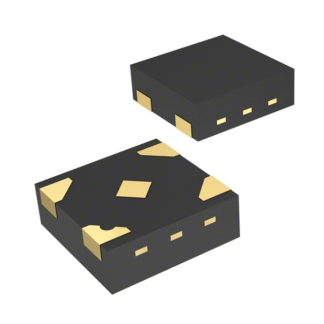
The 74AXP1G00GXH from Nexperia is a single, low-power, 2-input NAND gate. It features Schmitt-trigger action on all inputs, making it tolerant of slower input rise and fall times. This device is designed for very low static and dynamic power consumption across its wide supply voltage range of 0.7 V to 2.75 V.
Key electrical specifications include a low input capacitance of 0.5 pF (typical) and low output capacitance of 1.0 pF (typical). The typical power dissipation capacitance (CPD) is 2.5 pF at 1.2 V, and the quiescent current (ICC) is a maximum of 0.6 μA at 85 °C. It offers a maximum propagation delay of 3 ns at 2.5 V with a 5 pF load.
ESD protection is robust, exceeding 2 kV for HBM (Class 2) and 1000 V for CDM. Latch-up performance exceeds 100 mA per JESD 78 Class II. The device accepts input voltages up to 2.75 V and exhibits low noise overshoot and undershoot, less than 10% of VCC. The IOFF circuitry supports partial power-down mode operation.
This NAND gate is available in a 5-X2SON surface mount package with dimensions of 0.80 x 0.80 mm. It is specified for operation in temperatures ranging from -40 °C to +85 °C.
| Qty | Low | High |
|---|---|---|
| 1+ | $0.22 | $0.22 |
Estimated market price range - modelled values for guidance only, not live distributor offers.
0.7V to 2.75V.
5-X2SON (0.80x0.80) surface mount package.
-40°C to +85°C.
3 ns maximum at 2.5V supply with 5 pF load.
Exceeds 2 kV HBM (ANSI/ESDA/JEDEC JS-001 Class 2) and exceeds 1000 V CDM (JESD22-C101E).
Exceeds 100 mA per JESD 78 Class II.
Maximum 0.6 µA at 85°C.