

| Distributor | Stock | Pricing | MOQ | PKG | Lead Time | Date Code | On Order Quantity | On Order Delivery | |
|---|---|---|---|---|---|---|---|---|---|
|
10,000 pcs
|
10000 pcs | On Request | 1 | On Request | On Request | On Request | On Request | On Request |
| Category | |
| Manufacturer Name | |
| Current | |
| Input Logic Level | |
| Input Voltage | |
| Latch-up Performance | |
| Logic Type | |
| Max Propagation Delay @ V, Max CL | |
| Mounting Type | |
| Number of Circuits | |
| Number of Inputs | |
| Operating Temperature | |
| SVHC Present | |
| Supplier Device Package | |
| Voltage |
The Nexperia 74AUP2G00GXX is a low-power dual 2-input NAND gate designed for a wide supply voltage range from 0.8 V to 3.6 V. This device features Schmitt trigger action at all inputs, providing tolerance to slower input rise and fall times across the entire VCC range. It ensures very low static and dynamic power consumption, with a typical quiescent current of 0.9 μA.
The 74AUP2G00GXX offers high noise immunity and complies with various JEDEC standards, including JESD8-12, JESD8-11, JESD8-7, JESD8-5, and JESD8-B. The device is fully specified for partial power-down applications using IOFF circuitry, which disables the output to prevent damaging backflow current when powered down. It also provides robust ESD protection, exceeding 5000 V for HBM and 1000 V for CDM.
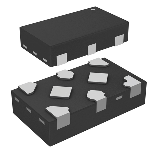
This NAND gate is available in multiple package options, including the 8-X2SON (1.35x0.8 mm) package, which is a plastic thermal enhanced extremely thin small outline package with no leads. The operating temperature range is specified from -40 °C to +125 °C. Its low propagation delay of 6.5 ns at 3.3V and 30pF makes it suitable for various digital logic applications requiring efficient and reliable performance.
| Qty | Low | High |
|---|---|---|
| 1+ | $0.22 | $0.22 |
Estimated market price range - modelled values for guidance only, not live distributor offers.
0.8 V to 3.6 V.
-40°C to +125°C.
8-X2SON (1.35 mm x 0.8 mm), surface mount; the datasheet also lists XSON8, VSSOP8, and XFDFN variants.
Dual 2-input NAND gate.
Two independent NAND gates, each with two inputs.
6.5 ns maximum at 3.3 V with 30 pF load.
Exceeds 5000 V HBM and 1000 V CDM; latch-up exceeds 100 mA per JESD78 Class II.