

| Distributor | Stock | Pricing | MOQ | PKG | Lead Time | Date Code | On Order Quantity | On Order Delivery | |
|---|---|---|---|---|---|---|---|---|---|
|
126 pcs
|
126 pcs | On Request | 1 | On Request | On Request | 12+ | On Request | On Request |
| Category | |
| Manufacturer Name | |
| Differential | |
| Frequency | |
| Input | |
| Lead Style | |
| Mounting Type | |
| Number of Circuits | |
| Number of Outputs | |
| Operating Temperature | |
| Output | |
| Ratio | |
| Supplier Device Package | |
| Tape & Reel | |
| Type | |
| Voltage |
The ZL40203LDG1 from Microchip Technology is a high-performance clock buffer designed for general-purpose clock distribution and low-jitter clock trees. It accepts differential or single-ended inputs, supporting logic levels such as LVPECL, LVDS, CML, HCSL, and LVCMOS. The device features on-chip input termination resistors and biasing for AC-coupled inputs.
This fanout buffer provides four precision LVPECL outputs and can operate at frequencies up to 750 MHz. It is designed for a supply voltage range of 2.375V to 3.465V and has a core current consumption of 62 mA. An on-chip Low Drop Out (LDO) regulator is included for superior power supply rejection. The ultra-low additive jitter of 40 fs RMS makes it suitable for demanding applications.
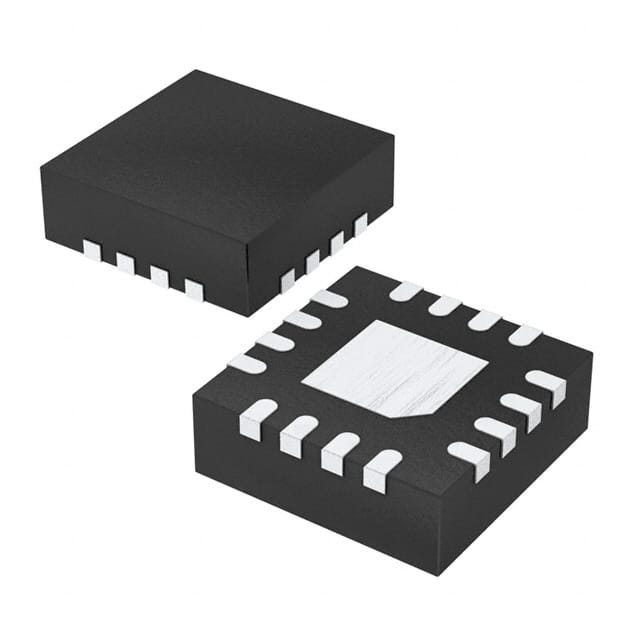
Packaged in a compact 16-VFQFN (3x3 mm) with surface mount termination, the ZL40203LDG1 is suitable for applications requiring precise clock signal distribution. Its operating temperature range is -40°C to 85°C.
Applications for the ZL40203LDG1 include logic translation, clock and data signal restoration, wired communications (OTN, SONET/SDH, GE, 10 GE, FC, 10G FC), PCI Express clock distribution, wireless communications, and high-performance microprocessor clock distribution.
| Qty | Low | High |
|---|---|---|
| 1+ | $4.44 | $4.44 |
Estimated market price range - modelled values for guidance only, not live distributor offers.
The ZL40203LDG1 operates at frequencies up to 750 MHz.
It accepts LVPECL, LVDS, CML, HCSL, and LVCMOS input logic levels.
The device operates from a supply voltage of 2.375V to 3.465V.
The ZL40203LDG1 operates within a temperature range of -40°C to 85°C.
The ZL40203LDG1 is available in a 16-VFQFN exposed pad package measuring 3x3 mm.