

| Distributor | Stock | Pricing | MOQ | PKG | Lead Time | Date Code | On Order Quantity | On Order Delivery | |
|---|---|---|---|---|---|---|---|---|---|
|
4,000 pcs
|
4000 pcs | On Request | 1 | On Request | On Request | On Request | On Request | On Request |
| Category | |
| Manufacturer Name | |
| Lead Spacing | |
| Mounting Type | |
| Number of I | |
| Number of LABs | |
| Number of Logic Elements | |
| Operating Temperature | |
| Supplier Device Package | |
| Supplier Package | |
| Total RAM Bits | |
| Voltage |
The XC7K325T-2FFG900I is a high-performance Field-Programmable Gate Array (FPGA) manufactured by Advanced Micro Devices, belonging to the Kintex-7 family. This device features a substantial logic capacity with 325,000 logic cells and 25,475 LABs, making it suitable for complex digital applications.
Key specifications include 840 DSP slices and 2,700 Kb of block RAM, supporting high processing power and flexibility. The operating frequency can reach up to 550 MHz, with a supply voltage range of 0.97V to 1.03V. It provides 500 I/O pins for versatile connectivity.
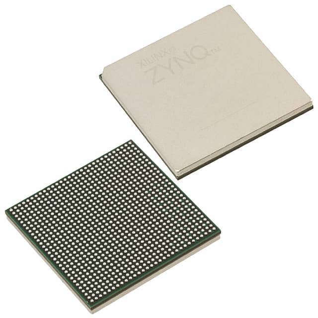
The XC7K325T-2FFG900I operates within a temperature range of -40°C to 100°C (TJ). It is housed in a 900-pin FC-BGA package, measuring 31x31, and utilizes surface mount technology for integration.
This FPGA is designed for advanced digital applications requiring high logic capacity, versatile I/O capabilities, and efficient power management. Its features make it suitable for applications demanding high processing power, flexibility, and reconfigurability.
| Qty | Low | High |
|---|---|---|
| 1+ | $21.20 | $21.20 |
Estimated market price range - modelled values for guidance only, not live distributor offers.
The XC7K325T-2FFG900I has 325,000 logic cells.
The XC7K325T-2FFG900I has 500 I/O pins.
The operating voltage range is 0.97V to 1.03V.
It is supplied in a 900-FCBGA (31x31) package.
The operating temperature range is -40°C to 100°C (TJ).
The operating frequency is up to 550 MHz.