

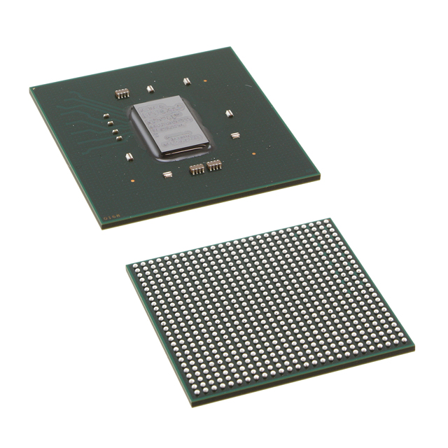
XC7K325T-2FFG676C The XC7K325T-2FFG676C is a high-performance FPGA from AMD. It features 326,080 logic elements, 400 I/O pins, and 16,404,480 RAM bits.
Mfr Part #:

XC7K325T-2FFG676C

Available from 2 distributors
Mfr Name: Xilinx
Xilinx
The XC7K325T-2FFG676C is a high-performance FPGA from AMD. It features 326,080 logic elements, 400 I/O pins, and 16,404,480 RAM bits.
✓ Total Stock: 1,500 pcs

XC7K325T-2FFG676C Available from 2 distributors

✓ Authorised
✓ Non-Authorised
Distributor Stock Pricing MOQ PKG Lead Time Date Code On Order Quantity On Order Delivery
Non-Authorised Inventory information
1,500 pcs
1500 pcs On Request 1 On Request On Request 17+ On Request On Request
Non-Authorised Inventory information
On Request On Request 1 On Request On Request On Request On Request On Request

XC7K325T-2FFG676C Specifications Quick View

Most important parameters for selection – full specs in datasheet.
Category
Manufacturer Name
Lead Spacing
Lead Style
Mounting Type
Number of I/O
Voltage Supply

XC7K325T-2FFG676C Description

Short technical summary and product information.

The XC7K325T-2FFG676C is a Field Programmable Gate Array (FPGA) manufactured by AMD. This device offers a high logic density with 326,080 logic elements and 25,475 LABs/CLBs, making it suitable for complex computational tasks. It provides extensive connectivity with 400 I/O pins and a substantial RAM capacity of 16,404,480 bits, supporting data-intensive applications.


The FPGA operates within a supply voltage range of 0.97V to 1.03V and has an operating temperature range of 0°C to 85°C (TJ). It is packaged in a 676FCBGA format and designed for surface mount applications. The XC7K325T-2FFG676C is RoHS3 compliant and REACH unaffected, meeting stringent environmental and safety standards.


AMD provides comprehensive development tools, including the Xilinx Vivado Design Suite, IP Integrator, and Xilinx SDK, to facilitate design and implementation. Its high logic density, extensive I/O capability, and large RAM capacity make it ideal for applications in high-performance computing, telecommunications, industrial automation, medical imaging, and aerospace and defense.

XC7K325T-2FFG676C Quick Information

Product Type: FPGA
Series: XC7K
Canonical Name: XC7K325T-2FFG676C Field Programmable Gate Array
Subcategory: Field Programmable Gate Array

XC7K325T-2FFG676C Compliance

RoHS Status: RoHS Compliant
Moisture Sensitivity Level (MSL): 1 Unlimited
REACH Status: REACH Unaffected
Lead Free: Yes

XC7K325T-2FFG676C Features

  • High logic density with 326,080 logic elements.
  • Extensive I/O capability with 400 pins.
  • Large RAM capacity of 16,404,480 bits.
  • Operates at 0.97V to 1.03V supply voltage.
  • Surface mountable in 676FCBGA package.

XC7K325T-2FFG676C Applications

  • Ideal for high-performance computing tasks.
  • Supports telecommunications data transmission.
  • Beneficial for industrial automation control.
  • Handles large data sets for medical imaging.
  • Suitable for aerospace and defense systems.

XC7K325T-2FFG676C FAQs

6 frequently asked questions generated from this part’s specifications.
What is the logic element count for the XC7K325T-2FFG676C FPGA?

The XC7K325T-2FFG676C FPGA has 326,080 logic elements.

How many I/O pins does the XC7K325T-2FFG676C have?

The XC7K325T-2FFG676C has 400 I/O pins.

What is the operating voltage range for the XC7K325T-2FFG676C?

The operating voltage range for the XC7K325T-2FFG676C is 0.97V to 1.03V.

What is the operating temperature range for the XC7K325T-2FFG676C?

The operating temperature range for the XC7K325T-2FFG676C is 0°C to 85°C (TJ).

What package type is the XC7K325T-2FFG676C supplied in?

The XC7K325T-2FFG676C is supplied in a 676FCBGA package.

What is the Moisture Sensitivity Level (MSL) for the XC7K325T-2FFG676C?

The Moisture Sensitivity Level (MSL) for the XC7K325T-2FFG676C is Level 4 (72 hours).

Home

Categories