

| Distributor | Stock | Pricing | MOQ | PKG | Lead Time | Date Code | On Order Quantity | On Order Delivery | |
|---|---|---|---|---|---|---|---|---|---|
|
323 pcs
|
323 pcs | On Request | 1 | On Request | On Request | On Request | On Request | On Request |
| Category | |
| Manufacturer Name | |
| Lead Style | |
| Mounting Type | |
| Number of I/O | |
| Supplier Device Package | |
| Voltage Supply |
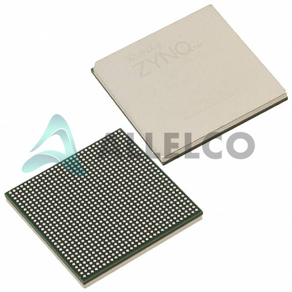
The XC7K325T-2FF676C is a Field Programmable Gate Array (FPGA) from Xilinx, part of the Kintex-7 family. This device is designed for high-performance applications, offering 326,080 logic elements and 25,475 LABs/CLBs. It provides 500 I/O pins for flexible interfacing.
With a total of 16,404,480 RAM bits, this FPGA is suitable for complex digital logic and signal processing tasks. The operating voltage ranges from 0.97V to 1.03V, and it operates within a temperature range of 0°C to 85°C (TJ).
The XC7K325T-2FF676C is housed in a 900-FCBGA package measuring 31x31 mm and is designed for surface mounting. Its specifications make it a versatile component for embedded systems and advanced electronic designs.
| Qty | Low | High |
|---|---|---|
| 1+ | $22.15 | $22.15 |
Estimated market price range - modelled values for guidance only, not live distributor offers.
The XC7K325T-2FF676C has 326,080 logic elements/cells.
The XC7K325T-2FF676C has 500 I/O pins.
The supply voltage range for the XC7K325T-2FF676C is 0.97V to 1.03V.
The XC7K325T-2FF676C comes in a 900-FCBGA (31x31) package.
The operating temperature range for the XC7K325T-2FF676C is 0°C to 85°C.
The XC7K325T-2FF676C has 25,475 LABs/CLBs.
The XC7K325T-2FF676C has 16,404,480 total RAM bits.