

| Distributor | Stock | Pricing | MOQ | PKG | Lead Time | Date Code | On Order Quantity | On Order Delivery | |
|---|---|---|---|---|---|---|---|---|---|
|
255 pcs
|
255 pcs | On Request | 1 | On Request | On Request | On Request | On Request | On Request |
| Category | |
| Manufacturer Name | |
| Operating Temperature | |
| SVHC Present | |
| Tape & Reel |
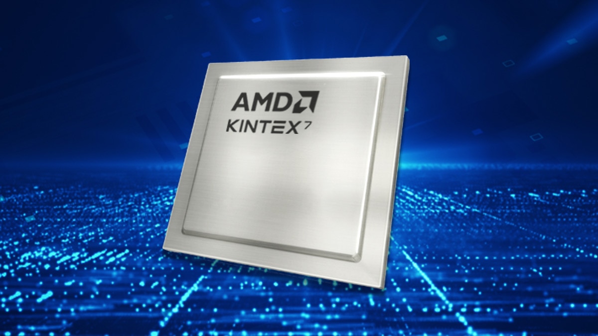
The Xilinx XC7K325T is a Field Programmable Gate Array (FPGA) belonging to the Kintex-7 family. This device is suitable for a wide range of embedded applications requiring flexible logic implementation.
Key specifications include support for speed grades -1 and -2, offering different performance characteristics. The operating temperature range for this FPGA is from 0 to 85°C, making it suitable for various environmental conditions.
Errata notifications exist for this device family. For Block RAM, when using the Built-In FIFO as a Synchronous FIFO with asynchronous reset, FIFO flag behavior may not be guaranteed after the first write. The recommended workaround is to synchronize the negative edge of reset to RDCLK/WRCLK. Asynchronous clocking for dual clock built-in FIFOs is not supported; use synchronous mode instead.
External memory interfaces also have errata. The Phaser block's "divide by two" mode for DDR3 and DDR2 is not operational between 303–399 MHz; it must be used in 1:1 mode, restricting the minimum supported DDR3/DDR2 memory clock frequency to 400 MHz. The PHY control block does not support a 2:1 PHY clock to memory controller clock ratio; use the 4:1 ratio in the Memory Interface Generator (MIG) tool for quarter rate solutions.
| Qty | Low | High |
|---|---|---|
| 1+ | $22.15 | $22.15 |
Estimated market price range - modelled values for guidance only, not live distributor offers.
The XC7K325T is available in speed grades -1 and -2.
The operating temperature range is 0 to 85°C.
When using the built-in FIFO as a synchronous FIFO with asynchronous reset, correct behavior of the FIFO flags cannot be guaranteed after the first write. The workaround is to synchronize the negative edge of reset to RDCLK/WRCLK. Asynchronous dual-clock FIFO operation is not supported.
The Phaser block divide-by-two mode is not operational for frequencies from 303 to 399 MHz. The Phaser block must be used in 1:1 mode, which restricts the minimum supported memory clock frequency to 400 MHz. The PHY control block does not support a 2:1 PHY clock to memory controller ratio.
Select the 4:1 PHY clock to memory controller clock ratio in the Memory Interface Generator tool to generate a quarter-rate solution.