

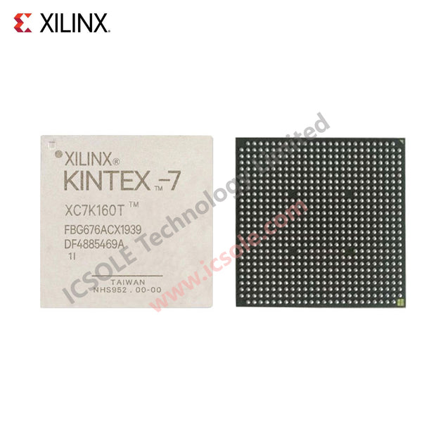
XC7K160T-1FBG676I The Xilinx XC7K160T-1FBG676I is a Kintex-7 series FPGA with 162,240 logic cells and 11,980,800 RAM bits. It features 400 I/O pins and operates within a voltage supply range of 0.95V to 1.05V.
Mfr Part #:

XC7K160T-1FBG676I

Available from 2 distributors
Mfr Name: Xilinx
Xilinx
The Xilinx XC7K160T-1FBG676I is a Kintex-7 series FPGA with 162,240 logic cells and 11,980,800 RAM bits. It features 400 I/O pins and operates within a voltage supply range of 0.95V to 1.05V.
Total Stock: 2,400 pcs

XC7K160T-1FBG676I Available from 2 distributors

Authorised
Non-Authorised
Distributor Stock Pricing MOQ PKG Lead Time Date Code On Order Quantity On Order Delivery
Non-Authorised Inventory information
2,200 pcs
2200 pcs On Request 1 On Request On Request 24+ On Request 2026-06-03 12:15:11
Non-Authorised Inventory information
200 pcs
200 pcs On Request 1 On Request On Request 21+ On Request On Request

XC7K160T-1FBG676I Specifications Quick View

Most important parameters for selection – full specs in datasheet.
Category
Manufacturer Name
Lead Style
Mounting Type
Number of I/O
Operating Temperature
SVHC Present
Supplier Device Package
Voltage Supply

XC7K160T-1FBG676I Description

Short technical summary and product information.

The Xilinx XC7K160T-1FBG676I is a high-performance FPGA from the Kintex-7 family, built on a 28nm process technology. It offers a significant improvement in price-performance compared to previous generations, enabling a new class of FPGAs.


This device features 162,240 logic cells and 12,675 CLBs, along with 11,980,800 total RAM bits. It provides 400 I/O pins and operates with a voltage supply range of 0.95V to 1.05V. The operating temperature range is -40°C to 100°C (TJ).


Designed for optimal system performance, the XC7K160T-1FBG676I boasts 2.9 Tb/s of I/O bandwidth and 5.3 TMAC/s DSP capabilities, while consuming 50% less power than previous generations. This makes it a programmable alternative to ASSPs and ASICs.


The FPGA is available in a 676-BBGA, FCBGA package and is designed for surface mounting. Its specifications make it suitable for a wide range of applications requiring high logic density, memory capacity, and I/O connectivity.

XC7K160T-1FBG676I Quick Information

Product Type: FPGA
Series: Kintex®-7
Canonical Name: Xilinx Kintex-7 XC7K160T-1FBG676I FPGA
Subcategory: Field Programmable Gate Array

XC7K160T-1FBG676I Compliance

RoHS Status: RoHS Compliant
Moisture Sensitivity Level (MSL): 1 Unlimited
REACH Status: REACH Unaffected

XC7K160T-1FBG676I Features

  • 162,240 logic cells and 11,980,800 RAM bits.
  • 400 I/O pins with 2.9 Tb/s bandwidth.
  • 0.95V to 1.05V operating voltage supply.
  • -40°C to 100°C operating temperature range.
  • 676-BBGA, FCBGA package for surface mounting.

XC7K160T-1FBG676I Applications

  • High-performance digital signal processing.
  • Complex logic and memory intensive designs.
  • System-on-chip (SoC) integration.
  • Advanced communication interfaces.

XC7K160T-1FBG676I FAQs

7 frequently asked questions generated from this part’s specifications.
What is the logic element count for the XC7K160T-1FBG676I?

The XC7K160T-1FBG676I has 162,240 logic elements.

How many I/O pins does the XC7K160T-1FBG676I offer?

The XC7K160T-1FBG676I offers 400 I/O pins.

What is the operating voltage range for this FPGA?

The operating voltage supply range for the XC7K160T-1FBG676I is 0.95 V to 1.05 V.

What is the package type and mounting method for the XC7K160T-1FBG676I?

The XC7K160T-1FBG676I comes in a 676-BBGA, FCBGA package and is designed for surface mounting.

What is the operating temperature range of the XC7K160T-1FBG676I?

The operating temperature range for the XC7K160T-1FBG676I is -40°C to 100°C (TJ).

What is the total RAM bit capacity of the XC7K160T-1FBG676I?

The XC7K160T-1FBG676I has a total RAM bit capacity of 11,980,800 bits.

What is the process technology used for the XC7K160T-1FBG676I?

The XC7K160T-1FBG676I is built on a 28 nm process technology.

Home
Account

Categories