

| Distributor | Stock | Pricing | MOQ | PKG | Lead Time | Date Code | On Order Quantity | On Order Delivery | |
|---|---|---|---|---|---|---|---|---|---|
|
3,013 pcs
|
3013 pcs | On Request | 1 | On Request | On Request | On Request | On Request | On Request |
| Category | |
| Manufacturer Name | |
| Halogen Free | |
| Mounting Type | |
| Number of I/O | |
| Voltage Supply |
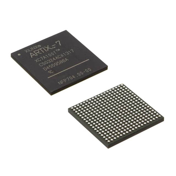
The Xilinx XC7A100T-2FG676I is an FPGA from the Artix-7 series, designed for embedded applications requiring programmable logic. This device features 101,440 logic elements and 7,925 logic blocks (LABs/CLBs), providing substantial capacity for complex digital circuit designs. It offers 210 user I/O pins for interfacing with other system components.
With 4,976,640 bits of onboard RAM, the XC7A100T-2FG676I supports data-intensive operations. The operating voltage range is 0.95V to 1.05V, and it operates within a junction temperature range of 0°C to 100°C. The component is housed in a 324-LFBGA, CSPBGA package, suitable for surface mounting.
This FPGA is based on 28nm SRAM process technology and integrates block RAM, digital signal processing (DSP) slices, and high-speed I/O cells. Its configurable logic blocks (CLBs/LABs) form the main programmable area, enabling reconfigurable logic and high-speed data processing capabilities for various embedded solutions and prototyping.
| Qty | Low | High |
|---|---|---|
| 1+ | $22.15 | $22.15 |
Estimated market price range - modelled values for guidance only, not live distributor offers.
The XC7A100T-2FG676I has 101,440 logic elements.
The XC7A100T-2FG676I provides 210 I/O pins.
The XC7A100T-2FG676I operates from 0.95V to 1.05V.
The XC7A100T-2FG676I is available in a 324-CSPBGA (15x15 mm) package.
The XC7A100T-2FG676I has 4,976,640 bits of total RAM.
The XC7A100T-2FG676I operates from 0°C to 100°C junction temperature.