

| Distributor | Stock | Pricing | MOQ | PKG | Lead Time | Date Code | On Order Quantity | On Order Delivery | |
|---|---|---|---|---|---|---|---|---|---|
|
2,260 pcs
|
2260 pcs | On Request | 1 | On Request | On Request | On Request | On Request | On Request |
| Category | |
| Manufacturer Name | |
| Lead Spacing | |
| Mounting Type | |
| Number of I | |
| Number of LABs | |
| Number of Logic Elements | |
| Operating Temperature | |
| Supplier Device Package | |
| Tape & Reel | |
| Technology | |
| Total RAM Bits | |
| Voltage |
The XC6SLX9-L1TQG144I is a high-performance Field Programmable Gate Array (FPGA) manufactured by Advanced Micro Devices. It belongs to the Spartan-6 LX family and is built using advanced 45nm technology, ensuring high performance and energy efficiency.
This FPGA features 9,152 logic elements (cells) and 715 Logic Array Blocks (LABs), providing ample resources for complex digital designs. It includes 589,824 RAM bits for substantial data storage and processing capabilities, along with 102 I/O pins for extensive connectivity options. The operating supply voltage ranges from 1.14V to 1.26V, optimized for low-power consumption.
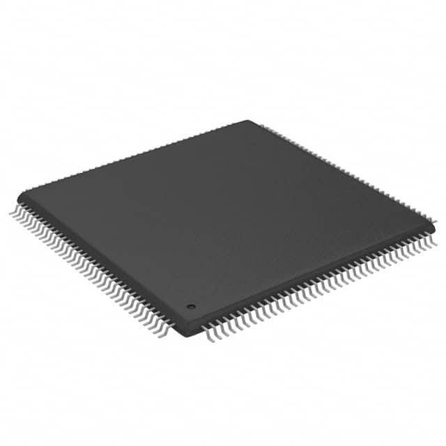
The XC6SLX9-L1TQG144I is packaged in a 144-pin TQFP (Thin Quad Flat Pack) with a 20x20mm body size, suitable for surface mount applications. This packaging ensures ease of integration into compact and high-density PCB designs. The operating temperature range is -40°C to 100°C (TJ).
Applications for this FPGA include embedded systems, digital signal processing (DSP), communication systems, automotive electronics, industrial automation, and consumer electronics. Advanced Micro Devices provides a comprehensive suite of development tools, including an IDE, simulation tools, and configuration tools, to support the design process.
| Qty | Low | High |
|---|---|---|
| 1+ | $21.20 | $21.20 |
Estimated market price range - modelled values for guidance only, not live distributor offers.
The supply voltage range is 1.14V to 1.26V.
It has 9,152 logic elements.
The XC6SLX9-L1TQG144I features 589,824 RAM bits.
There are 102 I/O pins available.
It is supplied in a 144-TQFP (20x20) package.
The operating temperature range is -40°C to 100°C (TJ).