

| Distributor | Stock | Pricing | MOQ | PKG | Lead Time | Date Code | On Order Quantity | On Order Delivery | |
|---|---|---|---|---|---|---|---|---|---|
|
7,244 pcs
|
7244 pcs | On Request | 1 | On Request | On Request | 19+ | On Request | On Request | |
|
4,520 pcs
|
4520 pcs | On Request | 1 | On Request | On Request | On Request | On Request | On Request | |
|
1,260 pcs
|
1260 pcs | On Request | 1 | On Request | On Request | 21+ | On Request | On Request | |
|
1,200 pcs
|
1200 pcs | On Request | 1 | On Request | On Request | On Request | On Request | On Request | |
|
4 pcs
|
4 pcs | On Request | 1 | On Request | On Request | On Request | On Request | On Request |
| Category | |
| Manufacturer Name | |
| Lead Style | |
| Mounting Type | |
| Number of I/O | |
| Operating Temperature | |
| SVHC Present | |
| Supplier Device Package | |
| Voltage Supply |
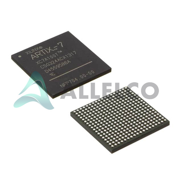
The XC6SLX9-2CSG324I is a Field Programmable Gate Array (FPGA) manufactured by AMD, belonging to the Spartan-6 LX family. This device offers 9152 logic elements and 715 logic array blocks (LABs/CLBs), with a total of 589824 RAM bits available for configuration.
It provides 200 input/output (I/O) pins, supporting a supply voltage range of 1.14V to 1.26V. The operating temperature range for this component is -40°C to 100°C (junction temperature).
The FPGA is designed for surface mounting and comes in a 324-LFBGA, CSPBGA package, specifically a 324-CSPBGA (15x15) variant. Its robust specifications make it suitable for various embedded applications requiring flexible logic implementation.
| Qty | Low | High |
|---|---|---|
| 1+ | $22.15 | $22.15 |
Estimated market price range - modelled values for guidance only, not live distributor offers.
The XC6SLX9-2CSG324I FPGA has 9152 logic elements.
The XC6SLX9-2CSG324I FPGA has a total of 589824 RAM bits.
The XC6SLX9-2CSG324I FPGA has 200 I/O pins.
The XC6SLX9-2CSG324I FPGA operates with a supply voltage between 1.14V and 1.26V.
The XC6SLX9-2CSG324I FPGA operates within a junction temperature range of -40°C to 100°C.
The XC6SLX9-2CSG324I FPGA is supplied in a 324-LFBGA, CSPBGA package, specifically a 324-CSPBGA (15x15).
Overheating can result from insufficient cooling, excessive power consumption due to overclocking, poor ventilation, or improper voltage settings.