

| Distributor | Stock | Pricing | MOQ | PKG | Lead Time | Date Code | On Order Quantity | On Order Delivery | |
|---|---|---|---|---|---|---|---|---|---|
|
535 pcs
|
535 pcs | On Request | 1 | On Request | On Request | On Request | On Request | On Request |
| Category | |
| Manufacturer Name | |
| Mounting Type | |
| Number of I | |
| Number of LABs | |
| Number of Logic Elements | |
| Operating Temperature | |
| Supplier Device Package | |
| Supplier Package | |
| Total RAM Bits | |
| Voltage |
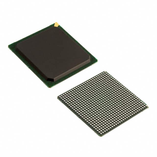
The XC6SLX100-2FGG676I is a field-programmable gate array (FPGA) manufactured by Advanced Micro Devices. It features 101,261 logic elements, 7,911 logic array blocks, and a total of 4,939,776 RAM bits. The device provides 480 I/O pins and operates within a voltage range of 1.14V to 1.26V. It is packaged in a 676-ball fine ball grid array (FBGA) with a 27x27 mm footprint and is designed for surface mounting.
This FPGA is suitable for embedded applications requiring high logic density and I/O flexibility. Its thermal operating range extends from -40°C to 100°C, making it suitable for a variety of industrial and consumer electronics environments. The package's surface-mount design facilitates integration into complex circuit boards, supporting high-speed digital logic functions.
The device complies with RoHS standards, although verification status is low, and has a Moisture Sensitivity Level (MSL) of 1, indicating unlimited reflow cycles. It is also unaffected by REACH regulations. The part number is referenced in the context of embedded system designs, digital signal processing, and high-density logic applications.
| Qty | Low | High |
|---|---|---|
| 1+ | $21.20 | $21.20 |
Estimated market price range - modelled values for guidance only, not live distributor offers.
The XC6SLX100-2FGG676I has 101,261 logic elements.
It is packaged in a 676-BGA package.
The device operates within a voltage range of 1.14V to 1.26V.
It has 480 I/O pins.