

| Distributor | Stock | Pricing | MOQ | PKG | Lead Time | Date Code | On Order Quantity | On Order Delivery | |
|---|---|---|---|---|---|---|---|---|---|
|
2,013 pcs
|
2013 pcs | On Request | 1 | On Request | On Request | 24+ | On Request | On Request |
| Category | |
| Manufacturer Name | |
| Mounting Type | |
| Number of I/O | |
| Voltage Supply |
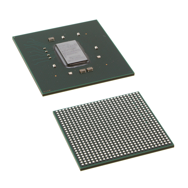
The XC5VLX85-2FF676I is a Field Programmable Gate Array (FPGA) from Xilinx, part of the Virtex-5 family. This device offers substantial programmable logic resources with 82,944 logic cells and 6,480 LABs/CLBs, complemented by 3,538,944 bits of total RAM. It provides extensive connectivity with 440 input/output pins.
Designed for high-density logic and extensive connectivity, this FPGA operates within a supply voltage range of 0.95V to 1.05V. The XC5VLX85-2FF676I is housed in a 676-pin FCBGA package and is suitable for surface mounting, making it compatible with modern PCB designs.
Its versatility makes it suitable for demanding applications across various industries. These include telecommunications, networking equipment, military and aerospace systems, industrial automation, and medical devices. Xilinx provides development tools like the ISE Design Suite and Vivado Design Suite to support engineers using this FPGA.
It has 82,944 logic elements.
440 I/O pins.
0.95V to 1.05V.
676FCBGA (Fine-Pitch Ball Grid Array).
3,538,944 bits.
6,480.