| Distributor | Stock | Pricing | MOQ | PKG | Lead Time | Date Code | On Order Quantity | On Order Delivery | |
|---|---|---|---|---|---|---|---|---|---|
|
2,000 pcs
|
2000 pcs | On Request | 1 | On Request | On Request | On Request | On Request | On Request |
| Category | |
| Manufacturer Name | |
| Lead Spacing | |
| Mounting Type | |
| Number of I | |
| Number of LABs | |
| Number of Logic Elements | |
| Operating Temperature | |
| Supplier Device Package | |
| Total RAM Bits | |
| Voltage |
The XC5VLX50T-2FF665I from Advanced Micro Devices is a Field Programmable Gate Array (FPGA) designed for complex digital logic applications. This device features 46080 logic elements and 3600 Logic Array Blocks (LABs), providing substantial capacity for custom logic implementation.
With 360 input/output (I/O) pins, the XC5VLX50T-2FF665I offers flexible connectivity for various system requirements. It includes 2,211,840 total RAM bits for on-chip data storage and processing. The operating voltage range is between 0.95V and 1.05V, suitable for power-sensitive applications.
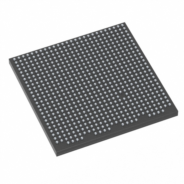
This FPGA is designed for surface mounting and comes in a 665-FCBGA (27x27) package. The operating temperature range is specified as -40°C to 100°C (TJ), ensuring reliable performance in demanding environments. Its RoHS3 compliance indicates adherence to environmental standards for electronic components.

| Qty | Low | High |
|---|---|---|
| 1+ | $21.20 | $21.20 |
Estimated market price range - modelled values for guidance only, not live distributor offers.
The XC5VLX50T-2FF665I has 46080 logic elements.
The XC5VLX50T-2FF665I has 360 I/O pins.
The operating voltage for the XC5VLX50T-2FF665I is between 0.95V and 1.05V.
The XC5VLX50T-2FF665I is supplied in a 665-FCBGA (27x27) package.
The operating temperature range for the XC5VLX50T-2FF665I is -40°C to 100°C (TJ).