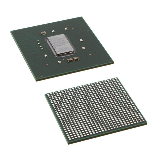
The Xilinx XC5VLX110-3FFG676C is a Field Programmable Gate Array (FPGA) designed for complex digital systems. It boasts a high logic density with 110,592 logic elements and 8,640 logic array blocks (LABs/CLBs).
This FPGA provides extensive connectivity with 440 I/O pins and substantial memory resources, featuring 4,718,592 total RAM bits. It operates within a supply voltage range of 0.95V to 1.05V and an ambient temperature range of 0°C to 85°C (TJ), ensuring reliable performance.
The XC5VLX110-3FFG676C is packaged in a 676FCBGA format and utilizes surface mount technology for efficient PCB integration. Its robust design makes it suitable for demanding applications in telecommunications, data centers, industrial automation, medical imaging, and aerospace.
Development for this FPGA is supported by AMD's comprehensive tool suite, including the Xilinx Vivado Design Suite and IP Integrator, facilitating efficient design, simulation, and verification.