

| Distributor | Stock | Pricing | MOQ | PKG | Lead Time | Date Code | On Order Quantity | On Order Delivery | |
|---|---|---|---|---|---|---|---|---|---|
|
362 pcs
|
362 pcs | On Request | 1 | On Request | On Request | On Request | On Request | On Request |
| Category | |
| Manufacturer Name | |
| Mounting Type | |
| Number of Gates | |
| Number of I | |
| Number of LABs | |
| Number of Logic Elements | |
| Operating Temperature | |
| Supplier Device Package | |
| Tape & Reel | |
| Technology | |
| Total RAM Bits | |
| Voltage |
The Xilinx XC3SD3400A-4FGG676C is part of the Spartan-3A DSP FPGA family, offering a high-performance DSP solution for high-volume applications. This FPGA features 53712 logic cells and 3.4 million gates, providing abundant logic resources for complex designs.
Key electrical specifications include an operating voltage range of 1.14V to 1.26V and 90nm technology. It offers 2.32 Mb of total RAM bits, including fast block RAM and efficient distributed RAM. The device supports DDR/DDR2 SDRAM up to 333 Mb/s and is compliant with 32-/64-bit, 33/66 MHz PCI standards.
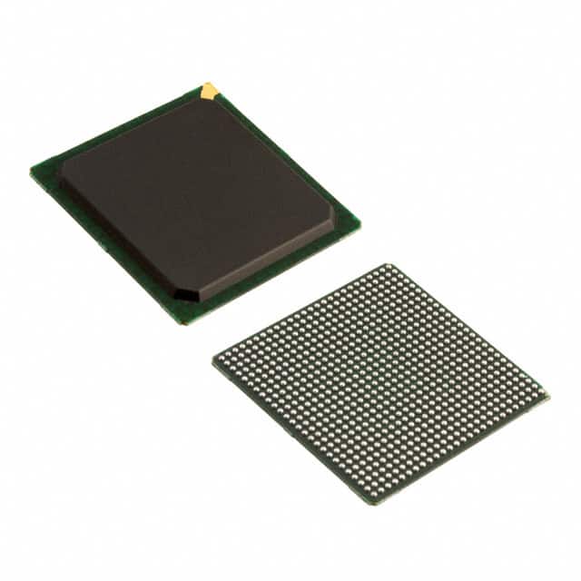
With 469 I/O pins, the XC3SD3400A-4FGG676C supports multi-voltage, multi-standard SelectIO interface pins, including LVCMOS, LVTTL, HSTL, and SSTL. It is packaged in a 676-FBGA (27x27) and is designed for surface mount applications. The operating temperature range is 0°C to 85°C (TJ).
This FPGA includes features like eight Digital Clock Managers (DCMs) for clock skew elimination and frequency synthesis, and a JTAG programming/debug port (IEEE 1149.1/1532). Configuration can be done via SPI serial Flash PROM, BPI parallel NOR Flash PROM, or Xilinx Platform Flash.
| Qty | Low | High |
|---|---|---|
| 1+ | $21.20 | $21.20 |
Estimated market price range - modelled values for guidance only, not live distributor offers.
The XC3SD3400A-4FGG676C has 53712 logic elements.
The XC3SD3400A-4FGG676C has 469 I/O pins.
The operating voltage for the XC3SD3400A-4FGG676C is between 1.14V and 1.26V.
The XC3SD3400A-4FGG676C is supplied in a 676-FBGA (27x27) package.
The speed grade of the XC3SD3400A-4FGG676C is -4.