

| Distributor | Stock | Pricing | MOQ | PKG | Lead Time | Date Code | On Order Quantity | On Order Delivery | |
|---|---|---|---|---|---|---|---|---|---|
|
139 pcs
|
139 pcs | On Request | 1 | On Request | On Request | On Request | On Request | On Request |
| Category | |
| Manufacturer Name | |
| Lead Spacing | |
| Mounting Type | |
| Number of I | |
| Number of LABs | |
| Number of Logic Elements | |
| Operating Temperature | |
| Supplier Device Package | |
| Total RAM Bits | |
| Voltage |
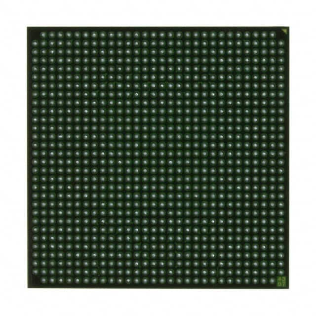
The Advanced Micro Devices XC2VP7-6FFG896C is a Field Programmable Gate Array (FPGA) from the Virtex-II Pro series. This component offers 396 input/output pins and 11088 logic elements, supported by 811008 total RAM bits.
Designed for surface mounting, it comes in an 896-BBGA, FCBGA package, specifically the 896-FCBGA (31x31) supplier device package. The operating voltage range is 1.425V to 1.575V, with an operating temperature range of 0°C to 85°C (TJ).
This FPGA is noted as 'Product Not Recommended For New Designs'. It is RoHS3 Compliant, has a Moisture Sensitivity Level (MSL) of 1, and is REACH Unaffected. These specifications make it suitable for various embedded applications where its features meet design requirements, though new designs should consider alternatives.
| Qty | Low | High |
|---|---|---|
| 1+ | $21.20 | $21.20 |
Estimated market price range - modelled values for guidance only, not live distributor offers.
The XC2VP7-6FFG896C has 11088 logic elements.
The XC2VP7-6FFG896C has 396 I/O pins.
The operating voltage for the XC2VP7-6FFG896C is between 1.425V and 1.575V.
The XC2VP7-6FFG896C is supplied in an 896-BBGA, FCBGA package.
The operating temperature range for the XC2VP7-6FFG896C is 0°C to 85°C (TJ).
The XC2VP7-6FFG896C is RoHS3 Compliant.
The Moisture Sensitivity Level (MSL) for the XC2VP7-6FFG896C is 1 Unlimited.