

| Distributor | Stock | Pricing | MOQ | PKG | Lead Time | Date Code | On Order Quantity | On Order Delivery | |
|---|---|---|---|---|---|---|---|---|---|
|
139 pcs
|
139 pcs | On Request | 1 | On Request | On Request | On Request | On Request | On Request |
| Category | |
| Manufacturer Name | |
| Lead Spacing | |
| Mounting Type | |
| Number of I | |
| Number of LABs | |
| Number of Logic Elements | |
| Operating Temperature | |
| Supplier Device Package | |
| Technology | |
| Total RAM Bits | |
| Voltage |
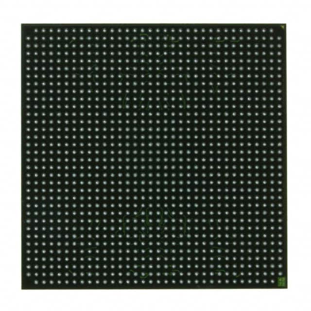
The Xilinx Virtex-II Pro FPGA, part number XC2VP50-6FFG1152I, is a powerful Field Programmable Gate Array designed for complex applications. This device offers 53136 logic cells and 5904 LABs, providing substantial programmable logic resources.
It supports up to 692 I/O pins and operates at a voltage range of 1.425V to 1.575V. The FPGA is built on a 0.13µm technology process and has a clock speed of 1200MHz. The operating temperature range is -40°C to 100°C (TJ).
Packaged in a 1152-pin FCBGA (Flip-Chip Ball Grid Array), this component is designed for surface mounting. The Virtex-II Pro architecture incorporates features like embedded multi-gigabit transceivers and PowerPC CPU blocks, making it suitable for telecommunication, wireless, networking, video, and DSP applications.
This FPGA is noted as 'Not Recommended For New Designs', indicating it is an older generation product. It is based on the Virtex-II Platform FPGA Technology and utilizes SRAM-based in-system configuration.
| Qty | Low | High |
|---|---|---|
| 1+ | $21.20 | $21.20 |
Estimated market price range - modelled values for guidance only, not live distributor offers.
The XC2VP50-6FFG1152I FPGA has 53,136 logic elements.
The XC2VP50-6FFG1152I has 692 I/O pins.
The operating voltage for the XC2VP50-6FFG1152I is between 1.425V and 1.575V.
The XC2VP50-6FFG1152I is supplied in a 1152-FCBGA (35x35) package.
The operating temperature range for the XC2VP50-6FFG1152I is -40°C to 100°C (TJ).
The XC2VP50-6FFG1152I has a clock speed of 1200MHz.