

| Distributor | Stock | Pricing | MOQ | PKG | Lead Time | Date Code | On Order Quantity | On Order Delivery | |
|---|---|---|---|---|---|---|---|---|---|
|
904 pcs
|
904 pcs | On Request | 1 | On Request | On Request | On Request | On Request | On Request |
| Category | |
| Manufacturer Name | |
| Lead Spacing | |
| Mounting Type | |
| Number of I | |
| Number of I/O | |
| Number of LABs | |
| Number of LABs/CLBs | |
| Number of Logic Elements | |
| Number of Logic Elements/Cells | |
| Operating Temperature | |
| Supplier Device Package | |
| Technology | |
| Total RAM Bits | |
| Voltage | |
| Voltage Supply |
The XC2VP40-6FFG1152I is a high-performance FPGA from AMD Xilinx's Virtex-II Pro and Virtex-II Pro X families. This device integrates multi-gigabit transceivers and PowerPC CPU blocks, making it suitable for telecommunication, wireless, networking, video, and DSP applications.
Key technical specifications include 43632 logic elements (4848 LABs/CLBs) and 3,538,944 total RAM bits. It offers 692 I/O pins and operates within a voltage supply range of 1.425V to 1.575V, with a nominal voltage of 1.5V. The operating temperature range is -40°C to 100°C (TJ).
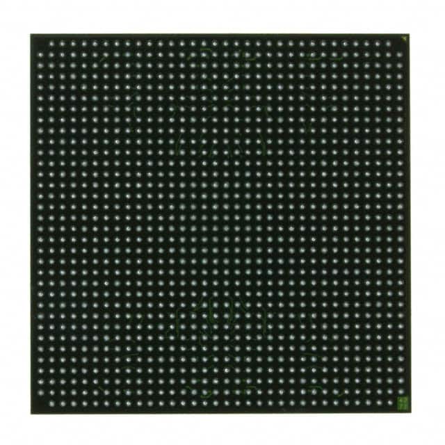
This FPGA utilizes a 0.13µm/90nm CMOS process technology and supports a maximum clock frequency of 1200MHz. It is packaged in a 1152-BBGA, FCBGA (1152-FCBGA (35x35)) and is designed for surface mounting.
The Virtex-II Pro architecture is optimized for high-performance designs and offers a flexible alternative to mask-programmed gate arrays. It supports various features like RocketIO™ Multi-Gigabit Transceivers and embedded PowerPC™ cores.
| Qty | Low | High |
|---|---|---|
| 1+ | $21.20 | $21.20 |
Estimated market price range - modelled values for guidance only, not live distributor offers.
The XC2VP40-6FFG1152I has 43632 logic elements.
The XC2VP40-6FFG1152I offers 692 I/O pins.
The operating voltage supply for the XC2VP40-6FFG1152I is 1.425V to 1.575V, with a nominal value of 1.5V.
The XC2VP40-6FFG1152I is supplied in a 1152-BBGA, FCBGA package.
The operating temperature range for the XC2VP40-6FFG1152I is -40°C to 100°C (TJ).
The XC2VP40-6FFG1152I uses a 0.13µm/90nm CMOS process technology.
The XC2VP40-6FFG1152I supports a maximum clock frequency of 1200MHz.