

| Distributor | Stock | Pricing | MOQ | PKG | Lead Time | Date Code | On Order Quantity | On Order Delivery | |
|---|---|---|---|---|---|---|---|---|---|
|
8,001 pcs
|
8001 pcs | On Request | 1 | On Request | On Request | On Request | On Request | On Request |
| Category | |
| Manufacturer Name | |
| Frequency | |
| Lead Spacing | |
| Mounting Type | |
| Number of I | |
| Number of LABs | |
| Number of Logic Elements | |
| Operating Temperature | |
| Supplier Device Package | |
| Technology | |
| Total RAM Bits | |
| Voltage |
The Xilinx XC2VP30-5FG676I is a high-performance FPGA from the Virtex-II Pro family, designed for demanding telecommunication, wireless, networking, video, and DSP applications. This device features 30,816 logic elements and 3,424 LABs, supported by 2,506,752 total RAM bits.
Key electrical specifications include an operating voltage range of 1.425V to 1.575V and a maximum frequency of 1050MHz. It offers 416 I/O pins and operates within a temperature range of -40°C to 100°C (TJ).
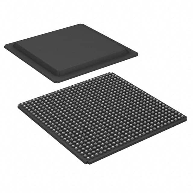
The XC2VP30-5FG676I is housed in a 676-FBGA (27x27) package and utilizes surface mount technology. The Virtex-II Pro architecture incorporates features like embedded Multi-Gigabit Transceivers and PowerPC CPU blocks, making it a powerful alternative to mask-programmed gate arrays for complex designs.
This FPGA is built on a 0.13µm CMOS process. It is noted as 'Not Recommended For New Designs' in the datasheet, suggesting it may be an older technology or superseded by newer alternatives.
| Qty | Low | High |
|---|---|---|
| 1+ | $21.20 | $21.20 |
Estimated market price range - modelled values for guidance only, not live distributor offers.
The operating temperature range is -40°C to 100°C (TJ).
The operating voltage is between 1.425V and 1.575V.
It has 416 I/O pins.
The package is a 676-FBGA (27x27).
The maximum operating frequency is 1050MHz.
It contains 30,816 logic elements.