

| Distributor | Stock | Pricing | MOQ | PKG | Lead Time | Date Code | On Order Quantity | On Order Delivery | |
|---|---|---|---|---|---|---|---|---|---|
|
723 pcs
|
723 pcs | On Request | 1 | On Request | On Request | On Request | On Request | On Request |
| Category | |
| Manufacturer Name | |
| Clock Frequency | |
| Data Rate | |
| Industrial Grade | |
| Lead Style | |
| Mounting Type | |
| Operating Temperature | |
| Operating Voltage |
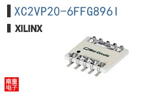
The Xilinx XC2VP20-6FFG896I is an FPGA from the Virtex-II Pro series, manufactured by Xilinx (now part of AMD). This device is built on a 0.13µm process technology and offers significant processing capabilities.
Key specifications include 20880 logic elements and 2320 logic blocks (LABs). It provides 1,622,016 total RAM bits for data storage and features 556 I/O pins supporting various interface standards like LVCMOS, LVTTL, and HSTL. The FPGA operates with a supply voltage between 1.425V and 1.575V and can function in temperatures ranging from -40°C to 100°C.
For high-speed serial communication, it includes RocketIO transceivers capable of data rates up to 3.125 Gbps. The device also supports DSP slices operating at up to 250 MHz and includes DCM (Digital Clock Manager) modules for clock management.
The XC2VP20-6FFG896I comes in an 896-FCBGA (Flip-Chip Ball Grid Array) package, designed for surface mounting. This FPGA is suitable for complex digital systems requiring high performance and flexibility.
| Qty | Low | High |
|---|---|---|
| 1+ | $22.15 | $22.15 |
Estimated market price range - modelled values for guidance only, not live distributor offers.
The FPGA contains 20880 logic elements.
It has 556 I/O pins.
The operating voltage range is 1.425V to 1.575V.
It is packaged in a 896-FCBGA (Fine-Pitch Ball Grid Array) for surface mount.
The typical maximum clock frequency for DSP slices is 250 MHz.
It operates from -40°C to 100°C.
It is built on a 0.13µm process technology.