
XC2VP20-5FGG676I
Advanced Micro Devices
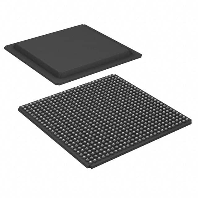
The Advanced Micro Devices XC2VP20-5FGG676I is an FPGA with 20880 logic elements and 404 I/O pins. It operates at 1.425V to 1.575V and is designed for surface mounting.


| Distributor | Stock | Pricing | MOQ | PKG | Lead Time | Date Code | On Order Quantity | On Order Delivery | |
|---|---|---|---|---|---|---|---|---|---|
|
8,000 pcs
|
8000 pcs | On Request | 1 | On Request | On Request | On Request | On Request | On Request |
| Category | |
| Manufacturer Name | |
| Lead Spacing | |
| Mounting Type | |
| Number of I | |
| Number of LABs | |
| Number of Logic Elements | |
| Operating Temperature | |
| Supplier Device Package | |
| Total RAM Bits | |
| Voltage |
The XC2VP20-5FG676I from Advanced Micro Devices is a Field Programmable Gate Array (FPGA) designed for high-performance applications. This device offers 20,880 logic elements and supports up to 404 I/O pins, making it suitable for complex digital designs.
It operates within a temperature range of -40°C to 100°C (TJ) and requires a supply voltage between 1.425V and 1.575V. The FPGA is housed in a 676-BGA package, specifically a 676-FBGA (27x27) variant, designed for surface mounting.
Key features include 1,622,016 total RAM bits and 2,320 LABs, providing substantial resources for logic implementation. The product is identified by the part number XC2VP20-5FG676I and is part of the Virtex-II Pro X family, though it is noted as 'Product Not Recommended For New Designs'.
| Qty | Low | High |
|---|---|---|
| 1+ | $21.20 | $21.20 |
Estimated market price range - modelled values for guidance only, not live distributor offers.
The XC2VP20-5FG676I has 20,880 logic elements.
The XC2VP20-5FG676I supports 404 I/O pins.
The operating voltage range is 1.425V to 1.575V.
The package type is 676-BGA, specifically a 676-FBGA (27x27).
The operating temperature is -40°C to 100°C (TJ).
The XC2VP20-5FG676I has 1,622,016 total RAM bits.
The XC2VP20-5FG676I contains 2,320 LABs.
