

| Distributor | Stock | Pricing | MOQ | PKG | Lead Time | Date Code | On Order Quantity | On Order Delivery | |
|---|---|---|---|---|---|---|---|---|---|
|
1,644 pcs
|
1644 pcs | On Request | 1 | On Request | On Request | On Request | On Request | On Request |
| Category | |
| Manufacturer Name | |
| Lead Spacing | |
| Mounting Type | |
| Number of Gates | |
| Number of I | |
| Number of LABs | |
| Operating Temperature | |
| Supplier Device Package | |
| Supplier Package | |
| Total RAM Bits | |
| Voltage |
The Advanced Micro Devices XC2V500-4FGG256C is a Field Programmable Gate Array (FPGA) designed for complex digital logic applications. This device offers a density of 500,000 gates and provides 172 input/output (I/O) pins, enabling extensive interfacing capabilities.
Key internal resources include 768 logic array blocks (LABs) and 589,824 bits of RAM, supporting sophisticated on-chip memory functions. The operating voltage for this FPGA ranges from 1.425V to 1.575V, with an operating temperature range of 0°C to 85°C (TJ).
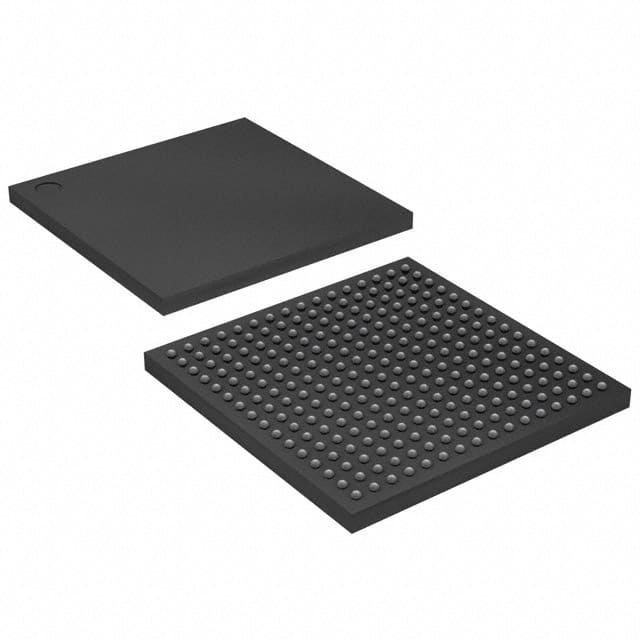
This component is housed in a 256-BGA (Ball Grid Array) package, specifically a 256-FBGA (Fine-Pitch Ball Grid Array) measuring 17x17 mm. It is designed for surface mounting, making it suitable for integration into various electronic assemblies.
The Virtex-II family, to which this part belongs, is known for its platform FPGA solution, offering high performance and flexible logic resources for demanding applications.
| Qty | Low | High |
|---|---|---|
| 1+ | $21.20 | $21.20 |
Estimated market price range - modelled values for guidance only, not live distributor offers.
The XC2V500-4FGG256C FPGA has 500,000 gates.
The XC2V500-4FGG256C has 172 I/O pins.
The XC2V500-4FGG256C features 589,824 total RAM bits.
The operating voltage for the XC2V500-4FGG256C is between 1.425V and 1.575V.
The operating temperature range is 0°C to 85°C (TJ).
The XC2V500-4FGG256C is supplied in a 256-FBGA (17x17) package.