

| Distributor | Stock | Pricing | MOQ | PKG | Lead Time | Date Code | On Order Quantity | On Order Delivery | |
|---|---|---|---|---|---|---|---|---|---|
|
579 pcs
|
579 pcs | On Request | 1 | On Request | On Request | On Request | On Request | On Request | |
| On Request | On Request | 1 | On Request | On Request | On Request | On Request | On Request |
| Category | |
| Manufacturer Name | |
| Mounting Type | |
| Number of I/O | |
| Operating Temperature |
The Xilinx XC2V250-4FG256I is a member of the Virtex-II family of Platform FPGAs. This device provides a high level of integration and performance for complex digital designs.
Key features include 250,000 logic elements, 256 I/O pins, and support for internal clock speeds up to 420 MHz. It also offers 16 dedicated 18x18 multipliers and substantial memory resources, including 1.5 Mb of distributed RAM and 16 blocks of 18 Kb SelectRAM.
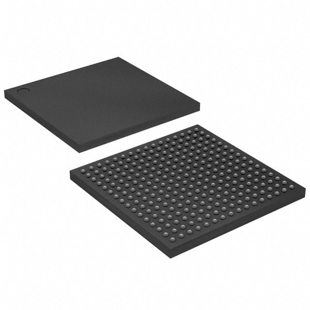
The XC2V250-4FG256I is packaged in a 256-pin Fine-Pitch Ball Grid Array (FG256) and is designed for surface mounting. Its operating temperature range is -40°C to 100°C.
This FPGA is suitable for a wide range of applications requiring high-density logic, flexible I/O, and high-speed processing capabilities.
| Qty | Low | High |
|---|---|---|
| 1+ | $4.72 | $4.72 |
Estimated market price range - modelled values for guidance only, not live distributor offers.
The logic array size is 250,000.
The XC2V250-4FG256I has 256 I/O pins.
The maximum internal clock speed is 420 MHz.
The XC2V250-4FG256I is in an FG256 package.
The operating temperature range is -40°C to 100°C.