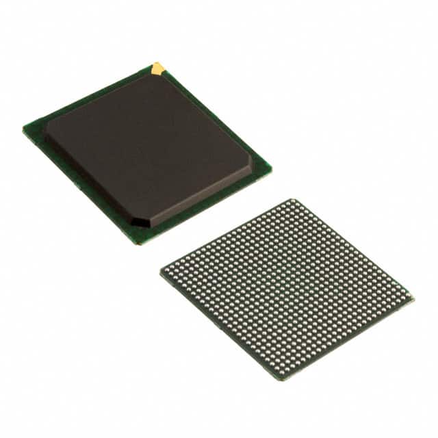
The Advanced Micro Devices XC2V1500-4FGG676I is a high-performance Field Programmable Gate Array (FPGA) from the Virtex-II Platform family. This device offers a density of 1.5 million gates and provides 392 input/output (I/O) pins, making it suitable for complex digital logic designs.
Key features include 884,736 total RAM bits and 1920 Logic Array Blocks (LABs), enabling significant on-chip memory and logic implementation. The FPGA operates within a voltage range of 1.425V to 1.575V and has an operating temperature range of -40°C to 100°C (TJ).
This component is designed for surface mount applications and comes in a 676-FBGA (27x27) package. Its specifications make it a versatile choice for various embedded systems and digital signal processing applications requiring flexible and reconfigurable logic.
The datasheet for this product, DS031 (v3.5) dated November 5, 2007, provides detailed information on its architecture, DC and switching characteristics, and pinout configurations for multiple package types.