

| Distributor | Stock | Pricing | MOQ | PKG | Lead Time | Date Code | On Order Quantity | On Order Delivery | |
|---|---|---|---|---|---|---|---|---|---|
|
8,000 pcs
|
8000 pcs | On Request | 1 | On Request | On Request | On Request | On Request | On Request |
| Category | |
| Manufacturer Name | |
| Mounting Type | |
| Number of Gates | |
| Number of I | |
| Number of LABs | |
| Number of Logic Elements | |
| Operating Temperature | |
| Supplier Device Package | |
| Tape & Reel | |
| Total RAM Bits | |
| Voltage |
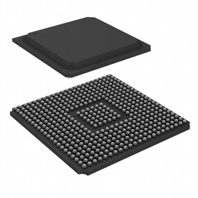
The Advanced Micro Devices XC2S400E-6FGG456C is a Field-Programmable Gate Array (FPGA) designed for high performance and abundant logic resources. This device offers 10,800 logic elements and 2,400 LABs, supporting up to 400,000 gates. It provides 329 user I/O pins and 163,840 total RAM bits.
Operating within a voltage range of 1.71V to 1.89V, the XC2S400E-6FGG456C has an operating temperature range of 0°C to 85°C (TJ). It is available in a 456-FBGA (23x23) package, specifically the 456-BBGA variant, and is designed for surface mount applications.
This FPGA family provides fast, predictable interconnect, making it suitable for applications requiring reliable timing across successive design iterations. It serves as an alternative to mask-programmed ASICs, avoiding initial costs and lengthy development cycles.
| Qty | Low | High |
|---|---|---|
| 1+ | $21.20 | $21.20 |
Estimated market price range - modelled values for guidance only, not live distributor offers.
The XC2S400E-6FGG456C FPGA has 10,800 logic elements.
The XC2S400E-6FGG456C FPGA has 329 user I/O pins.
The operating voltage range for the XC2S400E-6FGG456C FPGA is 1.71V to 1.89V.
The XC2S400E-6FGG456C FPGA is supplied in a 456-FBGA (23x23) package, also referred to as 456-BBGA.
The operating temperature range for the XC2S400E-6FGG456C FPGA is 0°C to 85°C (TJ).
The XC2S400E-6FGG456C FPGA has a total of 163,840 RAM bits.