

| Distributor | Stock | Pricing | MOQ | PKG | Lead Time | Date Code | On Order Quantity | On Order Delivery | |
|---|---|---|---|---|---|---|---|---|---|
|
3,200 pcs
|
3200 pcs | On Request | 1 | On Request | On Request | On Request | On Request | On Request |
| Category | |
| Manufacturer Name | |
| Lead Style | |
| Memory Size | |
| Mounting Type | |
| Operating Temperature | |
| Process | |
| Programmable Type | |
| Supplier Device Package | |
| Voltage |
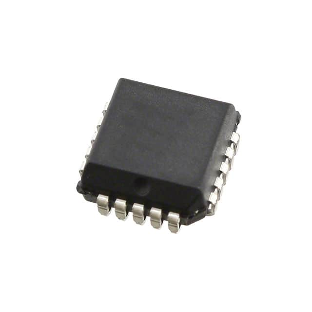
The Xilinx XC18V01PC20I is an in-system programmable 3.3V PROM from Advanced Micro Devices, designed for storing and reprogramming Xilinx FPGA configuration bitstreams. This device offers a memory size of 1Mb and supports dual configuration modes, including serial (up to 33 MHz) and parallel (up to 264 Mb/s at 33 MHz).
Key features include an endurance of 20,000 program/erase cycles and operation over the full industrial voltage and temperature range of -40°C to +85°C. The PROM supports IEEE Std 1149.1 boundary-scan (JTAG) for configuration initiation and features 5V tolerant I/O pins. It is available in a 20-PLCC (9x9) package, suitable for surface mounting.
This PROM is cascadable for storing longer or multiple bitstreams and utilizes a low-power advanced CMOS FLASH process. It provides a simple interface to the FPGA and offers 3.3V or 2.5V output capability. Design support is available using Xilinx Alliance and Foundation series software packages.
| Qty | Low | High |
|---|---|---|
| 1+ | $1.50 | $1.50 |
Estimated market price range - modelled values for guidance only, not live distributor offers.
The XC18V01PC20I operates within a voltage range of 3V to 3.6V.
The XC18V01PC20I is available in a 20-PLCC (9x9) package, specifically a 20-LCC (J-Lead).
The XC18V01PC20I has a memory size of 1Mb.
The XC18V01PC20I has an endurance of 20,000 Program/Erase Cycles.
Yes, the XC18V01PC20I supports IEEE Std 1149.1 boundary-scan (JTAG).
The operating temperature range for the XC18V01PC20I is -40°C to 85°C.
The XC18V01PC20I has a Surface Mount mounting type.