

| Distributor | Stock | Pricing | MOQ | PKG | Lead Time | Date Code | On Order Quantity | On Order Delivery | |
|---|---|---|---|---|---|---|---|---|---|
|
973 pcs
|
973 pcs | On Request | 1 | On Request | On Request | N/A | On Request | On Request |
| Category | |
| Manufacturer Name | |
| Channel Type | |
| Current | |
| Driven Configuration | |
| Gate Type | |
| Input Type | |
| Logic Voltage | |
| Mounting Type | |
| Number of Drivers | |
| Operating Temperature | |
| Propagation Delay | |
| Rise | |
| Supplier Device Package | |
| Voltage |
The UCC37325DGNR from Texas Instruments is a high-speed dual low-side power MOSFET driver. It delivers ±4A source and sink peak current, making it effective for driving MOSFETs at the Miller Plateau Region. The device features a Bi-CMOS output architecture and a unique BiPolar and MOSFET hybrid output stage for efficient current sourcing and sinking, even at low supply voltages.
Key electrical specifications include a supply voltage range of 4.5V to 15V, with typical rise and fall times of 20ns and 15ns respectively at a 1.8nF load. Propagation delay is rated at 35ns for rise and 25ns for fall. The input thresholds are based on TTL and CMOS, independent of the supply voltage, and offer wide input hysteresis for excellent noise immunity.
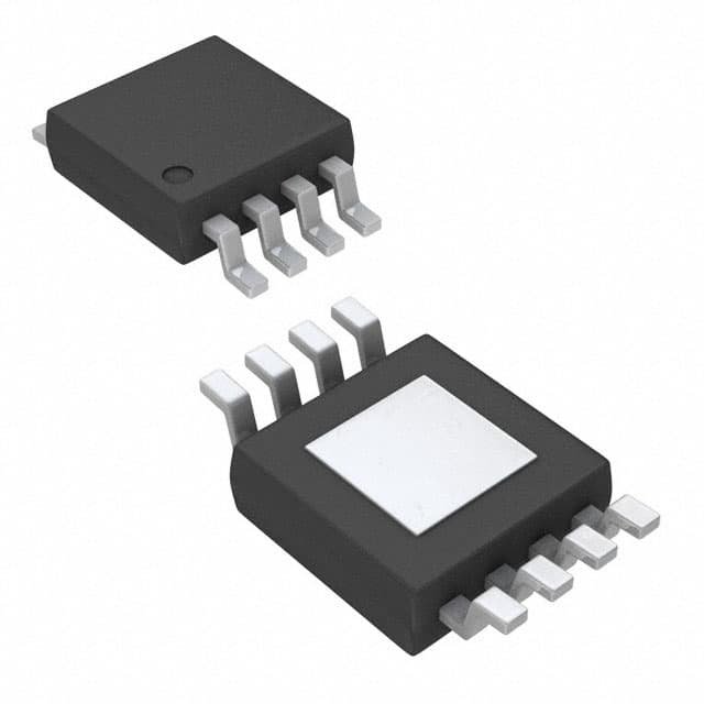
This driver is available in an 8-pin MSOP-PowerPAD package, which significantly lowers thermal resistance for improved long-term reliability. The industry-standard pin-out and TTL/CMOS inputs independent of supply voltage simplify integration into various designs. Applications include switch-mode power supplies, DC-DC converters, solar inverters, and motor control systems.
The UCC37325DGNR offers two independent channels, each capable of driving N-Channel or P-Channel MOSFETs. The input types include both inverting and non-inverting options, providing flexibility for different circuit configurations. Its low-side driven configuration is suitable for a wide range of power management applications.
| Qty | Low | High |
|---|---|---|
| 1+ | $0.37 | $0.37 |
Estimated market price range - modelled values for guidance only, not live distributor offers.
The supply voltage range is 4.5V to 15V.
The junction temperature range is -55°C to 150°C.
The device is available in 8-HVSSOP, 8-TSSOP, and 8-MSOP (0.118", 3.00mm Width) Exposed Pad packages.
The peak source and sink drive current is 4A at the Miller Plateau region.
Typical rise time is 20ns and fall time is 15ns at 1.8nF load.
The rise propagation delay is 35ns and fall propagation delay is 25ns.
The driver can drive both N-channel and P-channel MOSFETs.