

| Distributor | Stock | Pricing | MOQ | PKG | Lead Time | Date Code | On Order Quantity | On Order Delivery | |
|---|---|---|---|---|---|---|---|---|---|
|
1,540 pcs
|
1540 pcs | On Request | 1 | On Request | On Request | On Request | On Request | On Request |
| Category | |
| Manufacturer Name | |
| Current | |
| Frequency | |
| Gain | |
| Mounting Type | |
| Noise Figure | |
| P1dB | |
| RF Type | |
| Storage Temperature | |
| Supplier Device Package | |
| Tape & Reel | |
| Test Frequency | |
| Voltage |
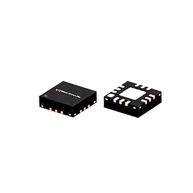
The Mini-Circuits TSS-53LNB3+ is a versatile low-noise amplifier (LNA) offering industry-leading performance across a broad frequency range of 500 MHz to 5 GHz. Utilizing E-PHEMT technology, this amplifier provides excellent noise figure and flat gain, making it suitable for a wide array of receiver applications.
A key feature of the TSS-53LNB3+ is its internal bypass switching capability. This allows the amplifier to handle both high and low signal levels effectively by bypassing the LNA when large signals are present, minimizing distortion. The amplifier boasts a typical noise figure of 1.5 dB at 2.0 GHz and a typical gain of 18.4 dB at 2 GHz, with ultra-flat gain characteristics.
Designed for ease of integration, the TSS-53LNB3+ requires minimal external matching components and comes in a compact 3 x 3mm, 12-lead MCLP package. This small footprint saves valuable space in dense system layouts. The amplifier is specified for full-band operation and is ideal for applications such as wireless base station systems, test and measurement systems, and multi-band receivers.
This model operates within a voltage range of 2.7V to 3.3V and has a typical current consumption of 42mA. The +Suffix indicates RoHS compliance.
| Qty | Low | High |
|---|---|---|
| 1+ | $0.98 | $0.98 |
Estimated market price range - modelled values for guidance only, not live distributor offers.
The TSS-53LNB3+ operates from 0.5 GHz to 5 GHz.
The typical noise figure is 1.5 dB at 2.0 GHz.
The typical gain is 18.4 dB at 2 GHz.
The P1dB is +15.1 dBm typical at 2.0 GHz.
The operating voltage is between 2.7V and 3.3V.
The TSS-53LNB3+ is supplied in a 12-MCLP (3x3mm) package.