

| Distributor | Stock | Pricing | MOQ | PKG | Lead Time | Date Code | On Order Quantity | On Order Delivery | |
|---|---|---|---|---|---|---|---|---|---|
|
960 pcs
|
960 pcs | On Request | 1 | On Request | On Request | 09+ | On Request | On Request |
| Category | |
| Manufacturer Name | |
| Control Features | |
| Current | |
| Input Voltage | |
| Mounting Type | |
| Number of Regulators | |
| Operating Temperature | |
| Output Configuration | |
| Output Type | |
| PSRR | |
| Protection Features | |
| Supplier Device Package | |
| Tape & Reel | |
| Voltage |
The TPS71825-12DRVR from Texas Instruments is part of the TPS718xx and TPS719xx families of dual-channel, low-dropout (LDO) linear regulators. These devices are designed for applications requiring high power-supply rejection ratio (PSRR), low noise, and fast start-up times.
Key electrical specifications include a typical dropout voltage of 230mV at 200mA, a low total quiescent current of 90µA with both LDOs enabled, and a low noise level of 70µV RMS/√Hz. The regulators offer independent enable pins for each LDO and are stable with 1µF ceramic capacitors. Protection features include over-current, over-temperature, and under-voltage lockout.
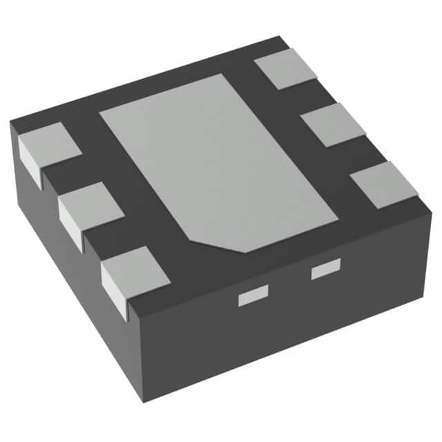
The TPS71825-12DRVR provides fixed output voltages of 2.5V and 1.2V, with an input voltage range of 2.7V to 6.5V. The output current capability is 200mA per channel. The device is available in a compact 2mm x 2mm 6-WSON package, suitable for space-constrained applications.
Applications for this regulator include digital cameras, camera modules, cellular phones, wireless LAN, Bluetooth devices, and handheld products. Its high PSRR and low noise make it suitable for sensitive analog circuits.
| Qty | Low | High |
|---|---|---|
| 1+ | $0.80 | $0.80 |
Estimated market price range - modelled values for guidance only, not live distributor offers.
The input voltage range is 2.7V to 6.5V.
The device provides fixed output voltages of 2.5V on LDO1 and 1.2V on LDO2.
Each output can deliver up to 200mA.
The typical dropout voltage is 230mV at 200mA load.
The typical quiescent current is 90µA with both LDOs enabled and no load.
The device is available in a 6-WSON (2x2) package and a 6-WDFN exposed pad package.
The operating junction temperature range is -40°C to 125°C.