

| Distributor | Stock | Pricing | MOQ | PKG | Lead Time | Date Code | On Order Quantity | On Order Delivery | |
|---|---|---|---|---|---|---|---|---|---|
|
6,400 pcs
|
6400 pcs | On Request | 1 | On Request | On Request | 22+ | On Request | On Request |
| Category | |
| Manufacturer Name | |
| Adjustable Output Voltage Range (Minimum/Maximum @ DCDC 1 and DCDC 2) | |
| Adjustable Output Voltage Range (Minimum/Maximum @ DCDC 3) | |
| Adjustable Output Voltage Range (Minimum/Maximum @ DCDC 4) | |
| Applications | |
| Input Voltage Range (Minimum/Maximum @ DCDC 4) | |
| Input Voltage Range (Minimum/Maximum) | |
| Mounting Type | |
| Number of Outputs | |
| Operating Temperature | |
| Output Current (Maximum @ DCDC 1) | |
| Output Current (Maximum @ DCDC 2) | |
| Output Current (Maximum @ DCDC 3) | |
| Output Current (Maximum @ DCDC 4) | |
| Output Voltage (@ DCDC 1) | |
| Output Voltage (@ DCDC 2) | |
| Output Voltage (@ DCDC 3) | |
| Output Voltage (@ DCDC 4) | |
| Storage Temperature | |
| Supplier Device Package | |
| Tape & Reel | |
| Voltage |
The Texas Instruments TPS65218B1RSLT is an integrated power management circuit designed for ARM Cortex-A8/A9 SoCs and FPGAs. This PMIC features multiple step-down converters and one buck-boost converter, providing a total of seven outputs to efficiently manage power requirements in complex systems.
Key electrical specifications include an input voltage range from 2.7 V to 5.5 V. The device offers adjustable output voltage ranges for its converters, with specific default voltages and maximum current capabilities detailed for DCDC1, DCDC2, DCDC3, and DCDC4. For instance, DCDC1 and DCDC2 default to 1.1 V and can be adjusted between 0.85 V and 1.675 V, each supporting up to 1.8 A. DCDC3 defaults to 1.2 V with an adjustable range of 0.9 V to 3.4 V, also supporting up to 1.8 A. DCDC4, a buck-boost converter, defaults to 3.3 V with an adjustable range of 1.175 V to 3.4 V and a maximum current of 1.6 A.
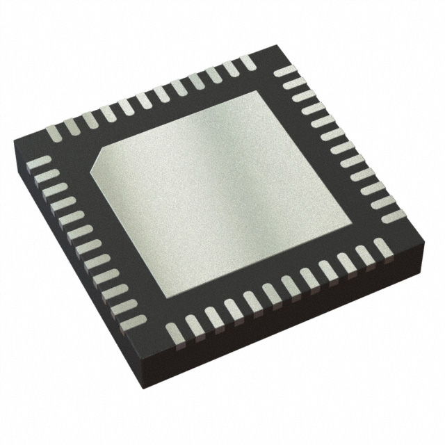
This PMIC operates within a temperature range of -40°C to 105°C. It is housed in a 48-VQFN (6x6) package with an exposed pad, suitable for surface mount applications. The TPS65218B1RSLT is noted as not recommended for new designs.
| Qty | Low | High |
|---|---|---|
| 1+ | $4.50 | $4.50 |
Estimated market price range - modelled values for guidance only, not live distributor offers.
The input voltage range is 2.7V to 5.5V.
The operating temperature range is -40°C to 105°C.
It is available in a 48-VQFN (6x6mm) package with exposed pad.
It has 7 outputs.
DCDC1, DCDC2, and DCDC3 can deliver up to 1.8A each, and DCDC4 up to 1.6A.
DCDC1 and DCDC2 can be adjusted from 0.85V to 1.675V, DCDC3 from 0.9V to 3.4V, and DCDC4 from 1.175V to 3.4V.
It is designed for ARM Cortex-A8/A9 SoCs and FPGAs.